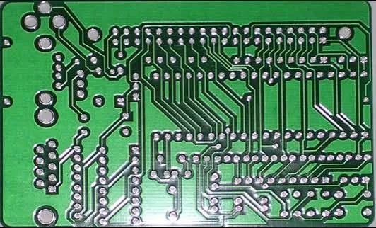
Large FPC ground opening designs often look perfect for EMI or flexibility on paper, but they frequently create serious issues during coverlay application and final assembly. Understanding the trade-offs in flexible PCB ground opening design helps avoid yield loss and reliability problems downstream.
Why Large Area Openings Increase Coverlay Processing Difficulty
Coverlay film is thin and flexible, but large copper openings make it prone to wrinkling, shifting, or poor adhesion. The bigger the ground opening, the harder it is to maintain uniform pressure and alignment during lamination.
Adhesive flow becomes uneven. You end up with voids, bubbles, or areas where the coverlay doesn't fully bond to the base material. This directly impacts yield.

Yield Risks in Production
Large continuous openings raise the chance of coverlay tearing or misalignment during punching or laser cutting. Once misaligned, exposed copper areas can cause shorts during assembly or in final use.
Why Factories Segment Ground Openings (Break Treatment)
Most experienced FPC manufacturers will break up large grounding openings into smaller segmented windows. This segmentation improves coverlay handling and registration accuracy.
The "bridges" of remaining copper or adhesive areas act as anchors that keep the coverlay stable during processing. Without them, the film can shift by 0.1 mm or more — enough to expose traces or create inconsistent insulation.

Manufacturing Perspective on Segmentation
Segmentation reduces material stress concentrations and makes the panel more stable through multiple lamination and routing steps. It also improves overall flatness of the finished flex circuit.
Impact on EMI Performance, Reliability, and Manufacturability
From an EMI standpoint, large ground openings can actually hurt performance if they create slot antennas or disrupt return current paths. Segmented designs with proper bridge placement often maintain better shielding effectiveness.
Reliability suffers when coverlay adhesion is compromised. Moisture ingress, delamination under thermal cycling, and mechanical fatigue all become more likely around oversized openings.
On the manufacturing side, large FPC ground opening designs increase inspection time and raise the probability of rework or scrap.
Real-World Trade-offs
Designers want maximum copper removal for flexibility, but factories need enough structure for repeatable processing. Finding the right balance is key to a successful flex PCB grounding opening implementation.
Ground Opening Design Optimization Suggestions
Limit individual opening size to 8–12 mm in the longest dimension when possible. Break larger areas into multiple smaller windows separated by 0.3–0.8 mm copper bridges, depending on current carrying needs.
Place bridges strategically — avoid critical signal paths and high-flex zones. Consider thermal relief patterns or grid-style openings for very large ground planes.
DFM Review Checklist for Ground Openings
• Check maximum opening size against fabricator capabilities
• Verify coverlay overlap on all sides of openings (minimum 0.1–0.2 mm recommended)
• Ensure no isolated copper islands inside openings
• Confirm bridge width supports both electrical and mechanical requirements
• Review registration tolerances for coverlay to copper features
Final Engineering Recommendations
FPC ground opening design requires balancing electrical, mechanical, and manufacturing needs. Oversized continuous openings often create more problems than they solve. Smart segmentation usually delivers better overall results in flexible PCB grounding opening applications.
Discuss large ground areas with your manufacturer early in the DFM stage. Their feedback on specific opening patterns can prevent costly revisions later. A well-designed grounding opening improves both producibility and long-term reliability.
Pay attention to these details — they separate designs that survive production from those that don't.