










PCB Specifications
| Parameter | Value | Parameter | Value |
|---|---|---|---|
| PCB Type | FR4 PCB | Quantity | 75 pcs |
| Layers | 4 Layers | Board Type | Panel PCB |
| Dimensions | 188 x 325 mm | Copper Weight | 1oz |
| Thickness | 1.6 mm | Min Track / Spacing | 6/6mil↑ |
| Surface Finish | ENIG (Immersion Gold) | Min Hole Size | 0.3mm↑ |
| Solder Mask | Green | Silkscreen | None |
| Stack-up | Custom | Impedance Control | Yes |
Manufacturing Timeline
Logistics Information
Key Manufacturing Processes
Manufacturing Summary
This production record covers 75 panels of a standard 4-layer FR4 PCB, each sized 188 x 325 mm with 1.6 mm thickness and 1 oz copper weight. Configured with a custom stackup to support impedance control, the boards utilized conventional 6/6 mil geometry along with 0.3 mm minimum hole sizes. Green solder mask was applied without silkscreen per the order requirements, complemented by an immersion gold ENIG surface finish for optimal conductivity and protection.
Manufacturing began with engineering review and stackup impedance engineering, including trace width compensation to achieve the target impedance values. Inner layer imaging, precise circuit etching, and high-pressure lamination established solid interlayer alignment. Subsequent processes involved solder mask application, electroless nickel deposition, and immersion gold deposition, followed by comprehensive TDR impedance testing and electrical testing to confirm compliance.
The 11-day production cycle yielded consistent results across all 75 panels, delivering dependable impedance controlled PCBs that meet the exacting standards for signal integrity and assembly reliability.
Explore More PCB Manufacturing Resources
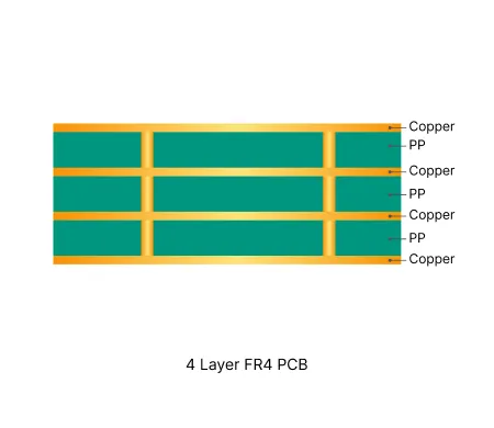
4 Layer FR4 PCB Manufacturing Insights
Standard multilayer solution offering practical routing density and controlled impedance for industrial and consumer electronics.

Multilayer FR4 PCB Engineering Queries Explained: Causes, Risks and Solutions
In-depth guide to the most frequent Engineering Queries (EQ) and DFM issues in Multilayer FR4 PCB (4/6/8+ layers) production. Real factory insights on stack-up confirmation, impedance control, copper balance, inner layer design, via treatment, registration, and practical prevention strategies.
Real Production Records
| Order ID | PCB Type | Layers | Dimensions | Solder Mask | Surface Finish | Quantity | Action |
|---|---|---|---|---|---|---|---|
| FR4-20260911-001 | FR4 PCB | 4 | 76.33 x 49.91 | Green | HASL Lead Free | 10 | View detail |
| FR4-20260819-043 | FR4 PCB | 10 | 157 x 140 | Blue | ENIG (Immersion Gold) | 100 | View detail |
| FR4-20260818-014 | FR4 PCB | 2 | 110.32 x 173.3 | Green | ENIG (Immersion Gold) | 200 | View detail |


