










PCB Specifications
| Parameter | Value | Parameter | Value |
|---|---|---|---|
| PCB Type | FR4 PCB | Quantity | 300 pcs |
| Layers | 4 Layers | Board Type | Panel PCB |
| Dimensions | 40 x 40 mm | Copper Weight | 1oz |
| Thickness | 1 mm | Min Track / Spacing | 6/6mil↑ |
| Surface Finish | ENIG (Immersion Gold) | Min Hole Size | 0.3mm↑ |
| Solder Mask | Blue | Silkscreen | White |
| Stack-up | Default | Impedance Control | No |
Manufacturing Timeline
Logistics Information
Key Manufacturing Processes
Manufacturing Summary
We completed a production run of 300 units of standard 4-layer FR4 PCBs arranged in panels. Each 40 × 40 mm board was built to 1.0 mm thickness with 1 oz copper weight, observing conventional 6/6 mil trace and spacing and 0.3 mm minimum hole size. Blue solder mask and white silkscreen were applied, followed by an immersion gold ENIG surface finish selected for its flat topography and long-term solderability on this moderate-volume order.
Manufacturing followed a disciplined sequence of inner-layer imaging, etching, and high-pressure lamination to maintain layer-to-layer registration across the panels. Nickel and gold deposition steps were monitored to achieve uniform coverage without excessive buildup on the 0.3 mm holes. After solder mask curing, batch AOI and 100 % electrical testing verified continuity and isolation on every panel during the 11.8-day schedule.
The finished panels exhibited stable dimensions and consistent surface quality, delivering reliable multilayer performance that aligned directly with the customer's assembly needs.
Explore More PCB Manufacturing Resources
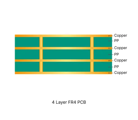
4 Layer FR4 PCB Manufacturing Insights
Standard multilayer solution offering practical routing density and controlled impedance for industrial and consumer electronics.

Multilayer FR4 PCB Engineering Queries Explained: Causes, Risks and Solutions
In-depth guide to the most frequent Engineering Queries (EQ) and DFM issues in Multilayer FR4 PCB (4/6/8+ layers) production. Real factory insights on stack-up confirmation, impedance control, copper balance, inner layer design, via treatment, registration, and practical prevention strategies.
Real Production Records
| Order ID | PCB Type | Layers | Dimensions | Solder Mask | Surface Finish | Quantity | Action |
|---|---|---|---|---|---|---|---|
| FR4-20260911-001 | FR4 PCB | 4 | 76.33 x 49.91 | Green | HASL Lead Free | 10 | View detail |
| FR4-20260819-043 | FR4 PCB | 10 | 157 x 140 | Blue | ENIG (Immersion Gold) | 100 | View detail |
| FR4-20260818-014 | FR4 PCB | 2 | 110.32 x 173.3 | Green | ENIG (Immersion Gold) | 200 | View detail |


