










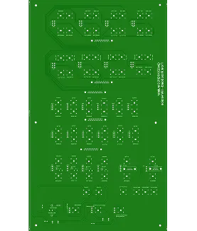
PCB Specifications
| Parameter | Value | Parameter | Value |
|---|---|---|---|
| PCB Type | FR4 PCB | Quantity | 10 pcs |
| Layers | 4 Layers | Board Type | Panel PCB |
| Dimensions | 319.5 x 545 mm | Copper Weight | 2oz |
| Thickness | 1.6 mm | Min Track / Spacing | 6/6mil↑ |
| Surface Finish | HASL Lead Free | Min Hole Size | 0.3mm↑ |
| Solder Mask | Green | Silkscreen | White |
| Stack-up | Default | Impedance Control | No |
Manufacturing Timeline
Logistics Information
Key Manufacturing Processes
Manufacturing Summary
This 4-layer FR-4 board, sized 319.5 × 545 mm with 2 oz copper on inner and outer layers and 1.6 mm finished thickness, was produced in a 10-piece run using KB-6165F material. The design incorporated laser-drilled blind vias with diameters adjusted from the original 0.2/0.3/0.4 mm to 0.15 mm, alongside a standard 6 mil line/space geometry and lead-free HASL surface finish. Panelization used a 1×1 configuration with 4 mm process edges on left and right sides, and the order required full mechanical forming with no impedance control or back-drilling.
DFM review focused on stackup verification for the target board and copper thickness tolerances, along with confirmation of the laser blind hole sizing adjustments and multi-layer drill pattern. Original 1-2 and 2-4 drill files contained overlapping, connecting, and closely spaced holes that behaved as effective 1-4 through vias in affected areas; production proceeded according to the provided drill data after customer confirmation, with no deletions applied to avoid unintended design changes. Process edge additions including production numbering and random tooling holes/optical fiducials with copper fill were also verified. Incoming material count was noted at 6 panels against the expected 10.
The boards completed 100% flying probe testing with no resin plugging required. All parameters met specifications within tolerance, delivering consistent registration and surface quality suitable for subsequent assembly despite the large panel dimensions and blind via modifications.
Explore More PCB Manufacturing Resources
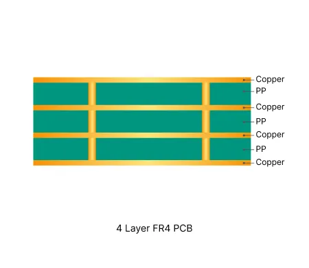
4 Layer FR4 PCB Manufacturing Insights
Standard multilayer solution offering practical routing density and controlled impedance for industrial and consumer electronics.

Multilayer FR4 PCB Engineering Queries Explained: Causes, Risks and Solutions
In-depth guide to the most frequent Engineering Queries (EQ) and DFM issues in Multilayer FR4 PCB (4/6/8+ layers) production. Real factory insights on stack-up confirmation, impedance control, copper balance, inner layer design, via treatment, registration, and practical prevention strategies.
Real Production Records
| Order ID | PCB Type | Layers | Dimensions | Solder Mask | Surface Finish | Quantity | Action |
|---|---|---|---|---|---|---|---|
| FR4-20261009-004 | FR4 PCB | 1 | 58.85 x 65.86 | Green | HASL Lead Free | 50 | View detail |
| FR4-20261007-048 | FR4 PCB | 2 | 99.04 x 75.87 | Matte Black | HASL Lead Free | 15 | View detail |
| FR4-20261007-047 | FR4 PCB | 2 | 92.84 x 72.52 | Green | HASL Lead Free | 5 | View detail |


