










PCB Specifications
| Parameter | Value | Parameter | Value |
|---|---|---|---|
| PCB Type | FR4 PCB | Quantity | 100 pcs |
| Layers | 8 Layers | Board Type | Panel PCB |
| Dimensions | 88.4 x 90.2 mm | Copper Weight | 1oz |
| Thickness | 1 mm | Min Track / Spacing | 6/6mil↑ |
| Surface Finish | ENIG (Immersion Gold) | Min Hole Size | 0.3mm↑ |
| Solder Mask | Green | Silkscreen | White |
| Stack-up | Custom | Impedance Control | No |
| Blind/Buried Vias | Yes |
Manufacturing Timeline
Logistics Information
Key Manufacturing Processes
Manufacturing Summary
This 8-layer HDI FR-4 board (88.4 × 90.2 mm, 1.0 mm finished thickness) was produced in a batch of 400 pieces (100 sets) using Shengyi S1000-2M TG170 material with 1 oz copper on inner and outer layers. The design included 0.3 mm holes, 6 mil line width/space, ENIG surface finish (2U"), blind vias, and resin-plugged vias on a 2×2 customer panel with V-CUT and routing. Production followed a 25-day lead time with 100% flying probe testing and delivery of electrical test reports plus quality certificates.
DFM review addressed several HDI-specific challenges. Low copper density on L3 and L6 was noted as a lamination risk that could lead to resin starvation or delamination; stack-up was designed from available materials and confirmed. Blind via pads at 0.127 mm for laser drilling and associated solder mask openings were verified against standard HDI PCB practices. NSMD BGA pads were processed per Gerber to improve pad adhesion and reduce cratering risk. Silk screen character frames in the BGA area were reviewed for component seating. Panelization details including V-CUT remaining thickness, angle, stamp hole combination, and process edge geometry were clarified and optimized to maintain panel strength during handling and depanelization.
All files and production parameters were confirmed before release. The completed boards met electrical, dimensional, and reliability requirements with consistent via filling and plating. For detailed resolution of the low copper density and laser via challenges in this HDI build, refer to the related engineering case.
Explore More PCB Manufacturing Resources
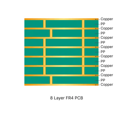
8 Layer FR4 PCB Manufacturing Insights
Discover how AIVON manufactures 8 Layer FR4 PCBs, including advanced multilayer structures, signal integrity requirements, impedance control, fabrication processes, manufacturing challenges, and real production experience from customer orders.

How to Avoid Common Engineering Queries in Multilayer FR4 PCB Design
Real multilayer FR4 PCB CAM review cases covering stack-up confirmation, impedance control, copper balance, via tenting, and edge clearance EQs. Discover practical DFM best practices for 4-layer and higher boards to reduce engineering queries, prevent warpage, and improve first-pass yield.
Real Production Records
| Order ID | PCB Type | Layers | Dimensions | Solder Mask | Surface Finish | Quantity | Action |
|---|---|---|---|---|---|---|---|
| FR4-20260819-043 | FR4 PCB | 10 | 157 x 140 | Blue | ENIG (Immersion Gold) | 100 | View detail |
| FR4-20260818-014 | FR4 PCB | 2 | 110.32 x 173.3 | Green | ENIG (Immersion Gold) | 200 | View detail |
| FR4-20260811-033 | FR4 PCB | 8 | 226.8 x 10⁹ | Green | ENIG (Immersion Gold) | 50 | View detail |


