










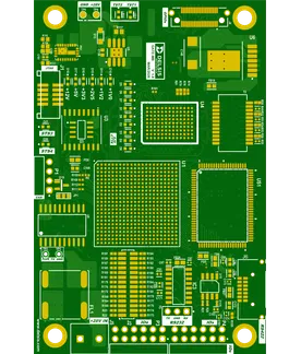
PCB Specifications
| Parameter | Value | Parameter | Value |
|---|---|---|---|
| PCB Type | FR4 PCB | Quantity | 5 pcs |
| Layers | 10 Layers | Board Type | Panel PCB |
| Dimensions | 95 x 62.37 mm | Copper Weight | 1oz |
| Thickness | 1.6 mm | Min Track / Spacing | 3/3mil |
| Surface Finish | ENIG (Immersion Gold) | Min Hole Size | 0.15mm |
| Solder Mask | Green | Silkscreen | White |
| Stack-up | Custom | Impedance Control | Yes |
Manufacturing Timeline
Logistics Information
Key Manufacturing Processes
Manufacturing Summary
This order consisted of five panelized 10-layer FR4 boards, each 95 x 62.37 mm with 1.6 mm thickness and 1 oz copper weight. The design incorporated a custom stackup, 3/3 mil trace and spacing, 0.15 mm minimum hole size, and impedance control. Engineering review focused on stackup impedance modeling and trace compensation to meet the specified electrical parameters before proceeding to material preparation and inner layer processing.
Layer stack alignment and high pressure lamination formed the 10-layer structure, after which green soldermask, white silkscreen, and immersion gold ENIG surface finish were applied. The ENIG process included electroless nickel deposition and immersion gold steps to provide a flat, reliable contact surface suitable for the fine features.
TDR impedance testing validated the controlled impedance lines, while comprehensive electrical testing confirmed circuit integrity. The executed processes delivered panels that matched the tight tolerances of this impedance controlled PCB configuration, supporting dependable performance in the intended application.
Explore More PCB Manufacturing Resources
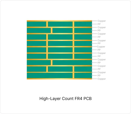
High-Layer Count FR4 PCB Manufacturing
These high-layer count FR4 PCB enable high-density interconnects while maintaining signal integrity and thermal reliability in computing and communication equipment.
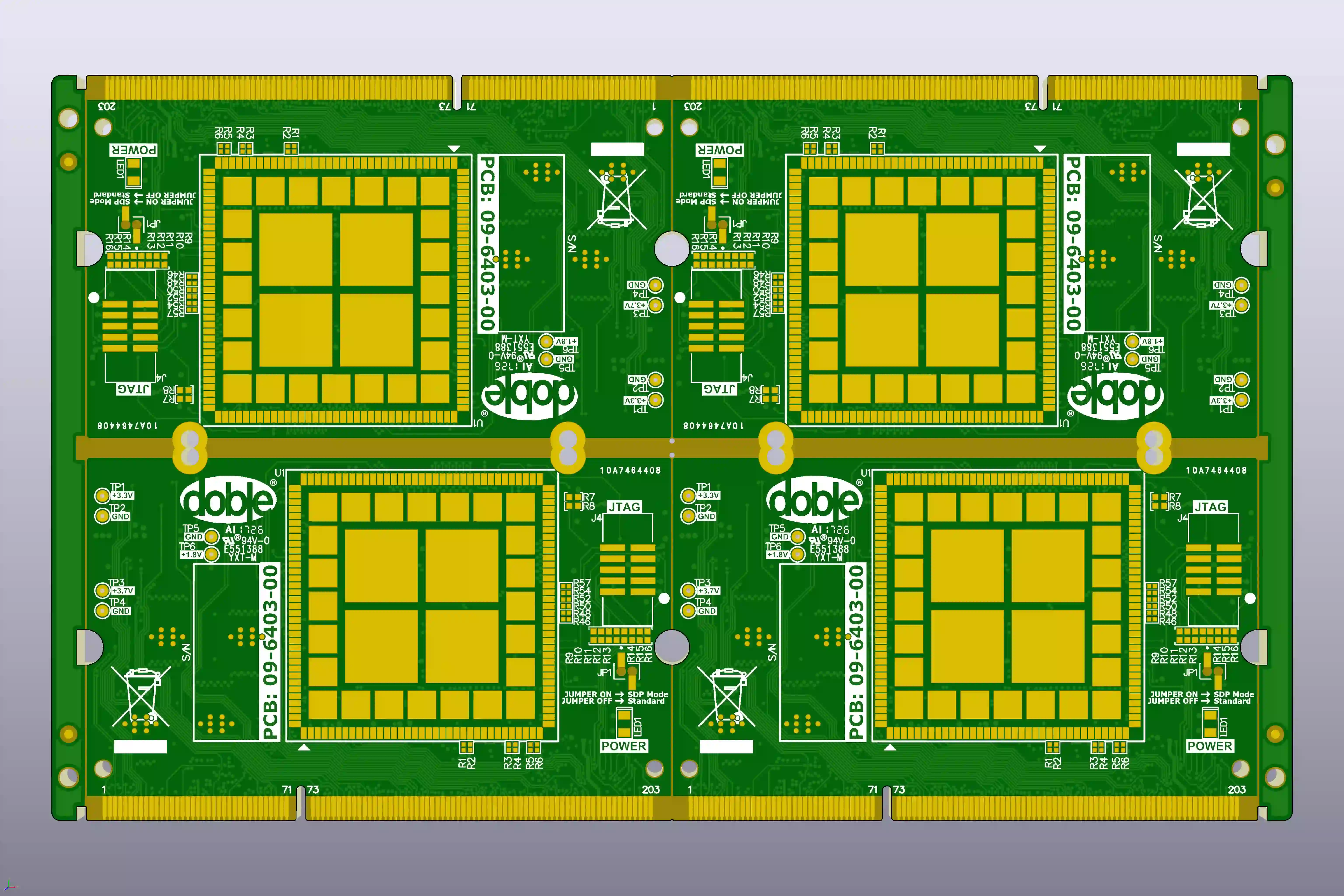
How to Resolve Gold Finger Bevel and Impedance EQs in 10-Layer PCBs
Real 10-layer FR-4 case study: how CAM engineers resolved gold finger bevel clearance, impedance mismatch, tight via spacing and plugging risks to prevent scrap and signal integrity failures.
Real Production Records
| Order ID | PCB Type | Layers | Dimensions | Solder Mask | Surface Finish | Quantity | Action |
|---|---|---|---|---|---|---|---|
| FR4-20260819-043 | FR4 PCB | 10 | 157 x 140 | Blue | ENIG (Immersion Gold) | 100 | View detail |
| FR4-20260818-014 | FR4 PCB | 2 | 110.32 x 173.3 | Green | ENIG (Immersion Gold) | 200 | View detail |
| FR4-20260811-033 | FR4 PCB | 8 | 226.8 x 10⁹ | Green | ENIG (Immersion Gold) | 50 | View detail |


