










PCB Specifications
| Parameter | Value | Parameter | Value |
|---|---|---|---|
| PCB Type | FR4 PCB | Quantity | 10 pcs |
| Layers | 4 Layers | Board Type | Single PCB |
| Dimensions | 124 x 25 mm | Copper Weight | 1oz |
| Thickness | 1.6 mm | Min Track / Spacing | 6/6mil↑ |
| Surface Finish | ENIG (Immersion Gold) | Min Hole Size | 0.3mm↑ |
| Solder Mask | Matte Black | Silkscreen | White |
| Stack-up | Default | Impedance Control | No |
Manufacturing Timeline
Logistics Information
Key Manufacturing Processes
Manufacturing Summary
For this order, we produced ten standard 4-layer PCBs, each measuring 124 x 25 mm with a thickness of 1.6 mm and 1 oz copper layers. The specifications called for a conventional 6/6 mil minimum track and spacing as well as 0.3 mm holes, without blind vias or impedance control. A matte black soldermask with white silkscreen lettering was chosen, topped with an immersion gold ENIG surface finish for durability and connectivity.
The manufacturing sequence started with engineering review and material preparation, followed by inner layer imaging, circuit etching, and precise layer stack alignment. High pressure lamination ensured solid multilayer construction before solder mask application. We then performed electroless nickel deposition and immersion gold deposition to create a flat, solderable ENIG surface.
Every board passed electrical testing for continuity and isolation. The complete process spanned 4.8 days and resulted in uniformly finished boards that offer reliable performance and an attractive matte appearance suited to the intended application.
This order also received positive feedback from the customer regarding the consistent quality and reliable delivery. View the full customer review→
Explore More PCB Manufacturing Resources
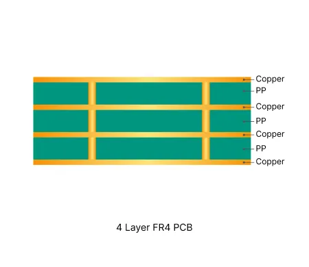
4 Layer FR4 PCB Manufacturing Insights
Discover how AIVON manufactures 4 Layer FR4 PCBs, including multilayer stackup design, layer alignment control, fabrication processes, manufacturing challenges, and real production experience from customer orders.

How to Avoid Common Engineering Queries in Multilayer FR4 PCB Design
Real multilayer FR4 PCB CAM review cases covering stack-up confirmation, impedance control, copper balance, via tenting, and edge clearance EQs. Discover practical DFM best practices for 4-layer and higher boards to reduce engineering queries, prevent warpage, and improve first-pass yield.
Real Production Records
| Order ID | PCB Type | Layers | Dimensions | Solder Mask | Surface Finish | Quantity | Action |
|---|---|---|---|---|---|---|---|
| FR4-20260819-043 | FR4 PCB | 10 | 157 x 140 | Blue | ENIG (Immersion Gold) | 100 | View detail |
| FR4-20260818-014 | FR4 PCB | 2 | 110.32 x 173.3 | Green | ENIG (Immersion Gold) | 200 | View detail |
| FR4-20260811-033 | FR4 PCB | 8 | 226.8 x 10⁹ | Green | ENIG (Immersion Gold) | 50 | View detail |


