










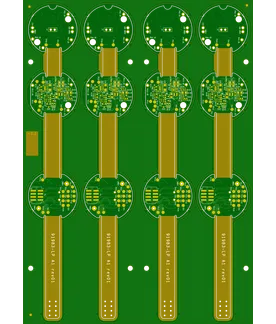
PCB Specifications
| Parameter | Value | Parameter | Value |
|---|---|---|---|
| PCB Type | Rigid-Flex PCB | Quantity | 25 pcs |
| Layers | 6 Layers | Board Type | Panel PCB |
| Dimensions | 209.3 x 148.6 mm | Copper Weight | 1OZ |
| Thickness | 1.2 mm | Min Track / Spacing | 6/6mil↑ |
| Surface Finish | ENIG (Immersion Gold) | Min Hole Size | 0.2mm |
| Solder Mask | Green | Silkscreen | White |
Manufacturing Timeline
Logistics Information
Key Manufacturing Processes
Manufacturing Summary
This order consisted of 25 six-layer rigid-flex PCB panels measuring 209.3 x 148.6 mm with a board thickness of 1.2 mm. The design specified 1 oz copper, a standard 6/6 mil trace and spacing, 0.2 mm minimum hole size, green solder mask, white silkscreen, and an immersion gold ENIG surface finish. These parameters required careful management during the flex-rigid lamination phase to achieve proper integration of the rigid and flexible zones without introducing stress concentrations.
Manufacturing proceeded through engineering review, material preparation, inner layer imaging, and circuit etching before high-pressure lamination and flex-rigid lamination. Solder mask was applied prior to the electroless nickel deposition and immersion gold deposition steps. Controlled depth routing then prepared the panel edges for separation.
Dynamic flex reliability testing validated the bending endurance of the flexible portions, while electrical testing verified all circuits. The 26-day production window permitted detailed process controls and multiple inspection points, resulting in a uniform set of panels ready for reliable field performance.
Explore More PCB Manufacturing Resources
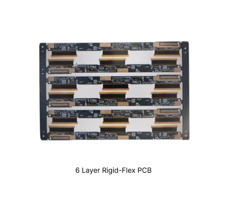
6 Layer Rigid-Flex PCB Manufacturing Insights
Discover how AIVON manufactures 6 Layer Rigid-Flex PCBs, including complex rigid-flex stackup design, layer transition control, reliability optimization, manufacturing challenges, and real production experience from customer orders.
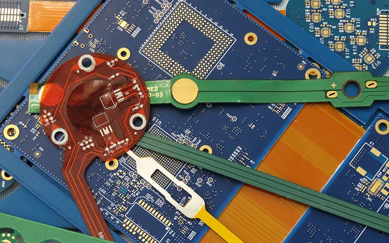
The Ultimate Guide to Rigid-Flex PCB Manufacturing: Mastering Complexity and Reliability at Scale
Navigate the full lifecycle of Rigid-Flex PCB Manufacturing. From solving high-density thermal challenges to scaling from prototype to production, master the tech and strategies for modern electronics.
Real Production Records
| Order ID | PCB Type | Layers | Dimensions | Solder Mask | Surface Finish | Quantity | Action |
|---|---|---|---|---|---|---|---|
| RFP-20260807-039 | Rigid-Flex PCB | 6 | 196 x 90 | Green | ENIG (Immersion Gold) | 30 | View detail |
| RFP-20260708-046 | Rigid-Flex PCB | 6 | 205 x 20 | Green | ENIG (Immersion Gold) | 125 | View detail |
| RFP-20260518-038 | Rigid-Flex PCB | 6 | 106.5 x 24 | Green | ENIG (Immersion Gold) | 5 | View detail |


