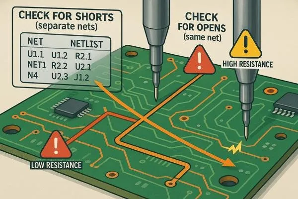
Most FPC electrical test failure reports come back with the same three codes: open, short, or resistance out of spec. The board looks fine under visual inspection. Then the flying probe or fixture hits it and the yield drops. That pattern is almost never random.
The majority of these failures originate in layout decisions that ignore how polyimide, adhesive, and copper actually behave under etch, lamination, and laser routing. Flexible PCB open short failure is less about process control and more about the design rules that were accepted at the start.
Open, Short, and Resistance Failures That Show Up on the Tester
Open is the most frequent. A trace that measured continuous on the artwork now reads infinite resistance. Short is next—two nets that should be isolated suddenly share continuity. Resistance abnormal is quieter but just as costly: the net is continuous, yet the measured value sits outside the ±10 % or ±20 % window the customer set.
These three categories are not independent. A trace that is already thinned by over-etch will often fail open after coverlay lamination stresses it. A residual copper filament that survived the etch will short two adjacent lines and also pull the resistance of both nets down. The tester simply reports the first limit that was crossed.
How Trace Geometry and Etch Factor Create Opens
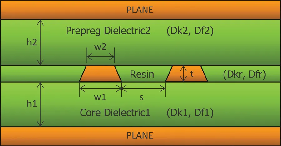
Copper on polyimide does not etch the way copper on FR-4 does. The etch factor is typically higher, and the adhesive layer under the copper can undercut more aggressively. When a designer draws a 50 µm line with a 50 µm space and assumes the finished width will stay 50 µm, the finished line often lands at 35–40 µm. That is already marginal for a ½-oz copper weight.
Sharp internal corners and neck-downs at pad entries make it worse. The etch attacks the corner first. After coverlay is laminated and the board is flexed once or twice during handling, the residual copper at that corner cracks. The electrical test sees an open. The crack is often invisible until the board is bent under a microscope.
Another common path to open is coverlay clearance that is too tight around a trace. The coverlay adhesive flows during the press cycle and can pull a thin trace sideways or create a local stress riser. When the board later sees thermal cycling or dynamic flex, the trace opens exactly at the coverlay edge.
Residual Copper and Registration Errors That Produce Shorts
Shorts on FPC are usually residual copper that the etch never fully cleared, or coverlay windows that are mis-registered relative to the copper. Both can be design-driven.
When minimum spacing is set at the absolute process limit (often 50 µm or less for fine-pitch flex), any local etch variation leaves a copper filament. That filament may survive the first few electrical tests and then bridge after the board is bent or after humidity exposure. The failure appears intermittent, which makes root-cause analysis painful.
Coverlay registration is the second major source. If the coverlay opening is drawn with zero clearance to a pad or to an adjacent trace, even a 50 µm registration shift will leave coverlay adhesive on copper or leave an unmasked copper finger that can short to a neighboring net during assembly. The electrical test catches the short before the board ever reaches the customer, but the yield is already lost.
Laser routing of the FPC outline can also create shorts. If copper is routed too close to the outline (less than 0.2 mm for many processes), the laser heat can redeposit carbonized material or leave a conductive edge that bridges two nets at the perimeter.
Distinguishing Layout-Driven Failures from Process Defects
When every board fails open at the same coordinate, the cause is almost always the artwork. Process variation is random in location and usually affects only a few percent of the panel. Systematic opens or shorts that map to the same net on every unit point back to a design feature—neck-down, acute angle, insufficient clearance, or a test-point that was never accessible.
Resistance failures that track the longest thin traces on the board are another layout signature. A 100 mm run of 40 µm copper will sit near the upper resistance limit even when the etch is perfect. Any additional width loss pushes it out of spec. Process control cannot fix a geometry that was drawn too aggressively.
The practical test is simple: if the same net fails on every panel from every lot, change the layout. If the failure rate jumps between lots or between different fabricators, look at etch chemistry, coverlay registration, or handling damage.
DFM Rules That Actually Reduce FPC Electrical Test Failure
Start with finished copper width, not artwork width. For ½-oz copper on polyimide, add at least 15–20 µm per side to compensate for etch factor if the target finished width is 50 µm. Many shops will tell you they can hold 50/50, but the electrical yield will suffer. 75/75 or 100/100 is far more robust for dynamic flex applications.
Eliminate acute internal angles. Replace them with 45° chamfers or full radius. The etch rate at a sharp corner is higher; the mechanical stress concentration is higher. Both increase open risk.
Keep copper at least 0.25 mm from the laser-routed outline unless the fabricator has qualified a tighter process. For punch routing the clearance can be smaller, but laser is the common method for complex outlines and it is unforgiving.
Coverlay openings need real clearance. A minimum 75–100 µm copper-to-coverlay edge is safer than the 50 µm that many drawings still carry. That extra margin absorbs registration tolerance and adhesive squeeze-out.
Test points must be large enough and accessible. A 0.3 mm pad under coverlay with a 0.15 mm opening is useless for flying-probe contact. Either open the coverlay fully or provide dedicated test pads outside the flex zone.
Finally, run a full netlist-driven DRC that includes the actual finished copper width and the coverlay layer, not just the artwork layers. Most layout tools default to artwork dimensions. The electrical test does not.
FPC electrical test failure is rarely a pure manufacturing mystery. Most open and short calls that survive multiple process lots map directly to geometry that was accepted during layout review. Tighten the etch compensation, open the clearances, and remove the stress concentrators. The test yield usually follows.