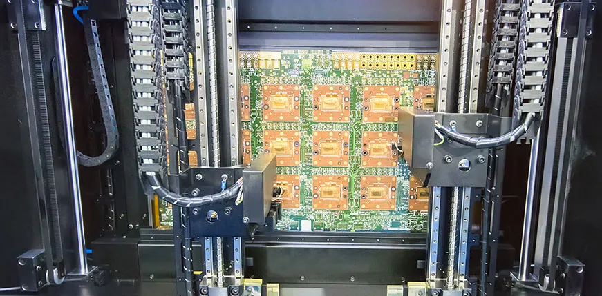
Bare Board Testing
Bare board testing is a critical step in the printed circuit board (PCB) manufacturing process, ensuring that the unpopulated board meets design specifications before components are assembled. This quality assurance technique identifies defects such as open circuits, short circuits, and manufacturing flaws early on, preventing costly rework or failures in the final product. For engineers, manufacturers, and hobbyists searching for information on bare board testing, this tag serves as a comprehensive resource, offering in-depth articles that cover everything from fundamental principles to advanced methodologies. Understanding bare board testing begins with recognizing its role in maintaining PCB integrity. Common methods include electrical testing like flying probe and fixture-based systems, as well as visual inspections using automated optical inspection (AOI) tools. By implementing these tests, professionals can achieve higher yield rates and comply with industry standards such as IPC-9252. Practical applications extend to various sectors, including consumer electronics, automotive, and aerospace, where reliability is paramount. For instance, best practices involve selecting the appropriate test strategy based on board complexity and production volume, which can significantly reduce time to market and minimize defects. This tag compiles expert insights on optimizing test setups, troubleshooting common issues, and integrating testing into automated workflows. Readers can find guidance on evaluating test equipment, interpreting results, and adapting techniques for high-density interconnect (HDI) boards. Whether you are troubleshooting a prototype or scaling up production, the articles here provide actionable strategies to enhance your PCB testing processes. Dive into the linked posts to gain a deeper understanding of specific testing protocols and real-world case studies that illustrate their effectiveness in ensuring robust electronic designs.
Technical Articles
Get in Touch
Send Message
- Products & Service
- Company
- About AIVON
- Contact
- News
- Blog
- Certification
-


- Payment
-


2026 AIVON.COM All Rights Reserved