Laser Drilling Defects
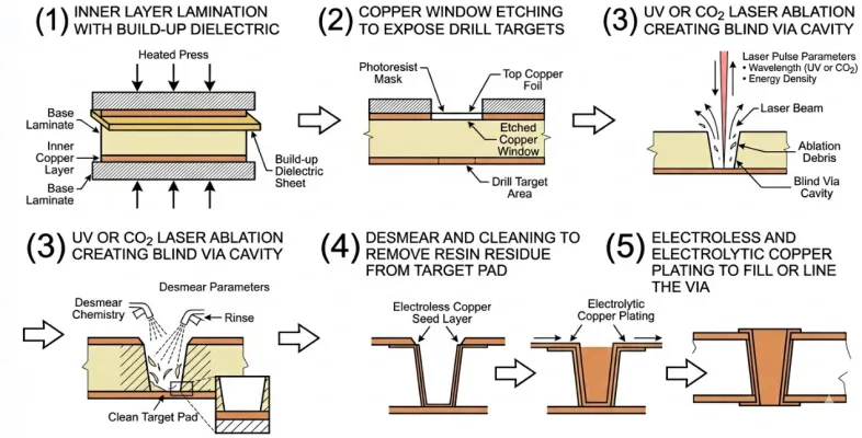
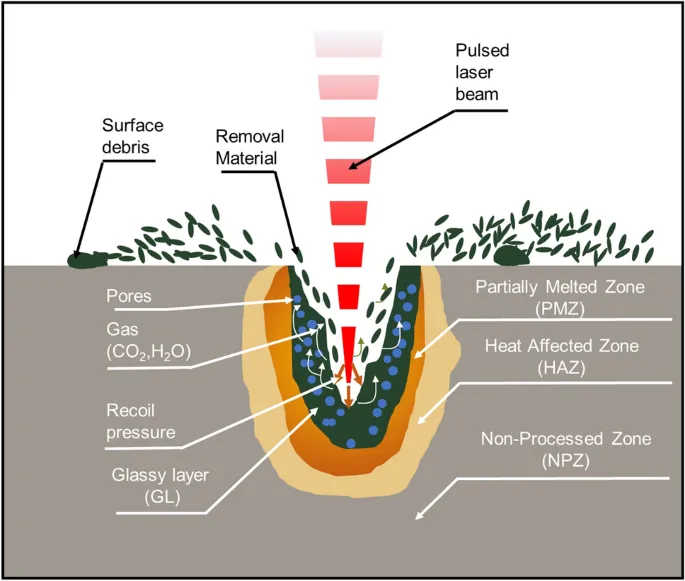
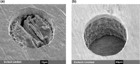
Laser drilling is a critical process in PCB manufacturing, enabling precise microvias and through-holes essential for high-density interconnects in modern electronics. However, defects in this process can compromise board integrity, leading to failures in functionality, reliability, and yield. This tag page on Laser Drilling Defects gathers expert insights into the most common issues encountered during laser ablation, such as taper irregularities, charring, delamination, and positional inaccuracies. By understanding these defects, engineers and manufacturers can better diagnose problems early in the production cycle, reducing costly rework and improving overall product quality. For those searching for solutions to laser drilling challenges, this collection offers practical guidance on root causes, including material incompatibilities, improper laser parameters, and equipment misalignment. Articles delve into best practices like optimizing pulse energy and beam focus to minimize thermal damage, as well as advanced techniques for defect detection using automated optical inspection and cross-sectional analysis. Whether you are troubleshooting a specific issue in multilayer PCBs or seeking preventive strategies for high-volume production, the resources here provide actionable steps to enhance process control and achieve consistent results. Professionals in electronics design and fabrication will find value in exploring the detailed case studies and technical discussions available under this tag. These pieces not only explain defect mechanisms but also share industry-tested methods for mitigation, helping you refine your manufacturing workflows. As laser technology evolves, staying informed on these topics ensures your projects meet stringent standards for performance and durability in applications ranging from consumer devices to aerospace systems.
Technical Articles
Get in Touch
Send Message
- Products & Service
- Company
- About AIVON
- Contact
- News
- Blog
- Certification
-


- Payment
-


2026 AIVON.COM All Rights Reserved