










PCB Tombstoning: Causes and Prevention in SMT Assembly
What This Video Covers
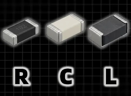
Tombstoning is an SMT reflow defect: one termination of a chip resistor, capacitor, or small inductor solders down while the other lifts until the part stands upright. This video explains the real mechanism—unbalanced solder force—not a mysterious "bad oven." When one pad melts earlier, carries more paste, or sits on a different copper mass, surface tension pulls harder on that end and tips the component.
Two factory drivers dominate. First, matching pad outlines does not guarantee matching paste volume. Stencil aperture, print release, and registration variation can load one pad more than the other. Second, two pads can look identical on the layout and still connect to different copper areas, so they heat and wet on different clocks.
Before release, check pad symmetry, copper connections, SMT stencil apertures, paste volume, and placement accuracy. Those checks belong in DFM, not after first-article inspection. The same risks show up on FR4 PCB prototypes and in turnkey PCB assembly for dense consumer, automotive, and industrial boards. Prevent the defect before the board reaches the oven.
Key Highlights
- Tombstoning happens when solder surface tension on one termination of a chip resistor, capacitor, or small inductor overwhelms the opposite pad, lifting the part upright during reflow.
- Matching pad outlines is not enough: stencil print variation changes paste volume, and unequal copper connections change how each pad heats and wets.
- Stop the defect before the oven by checking pad symmetry, copper attachments, stencil apertures, paste volume, and placement accuracy.
What Tombstoning Looks Like on a Finished Board
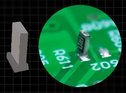
On a populated board, a tombstone is easy to miss until AOI or first power-up. A two-terminal chip part—most often an 0402 or 0201 resistor or capacitor, sometimes a small inductor—stands on one pad. One end has a fillet. The other end is in the air. Electrically that is an open or an intermittent joint. Mechanically it is a part that will not survive vibration, thermal cycling, or conformal coating without further damage.
The name is visual, not diagnostic. "Manhattan effect" and "drawbridging" describe the same force imbalance. The defect is most visible on lightweight chip packages because surface tension of molten solder can easily rotate a low-mass body. Larger 0805 and 1206 parts can still lift if paste volume or copper heat sinking is extreme, but the yield hit concentrates on small passives used in decoupling, pull-ups, and filter networks.
For engineering buyers, tombstoning is a first-article and NPI problem with a production tail. One upright 0201 on a prototype is a rework. The same pattern across a panel in PCB mass production is scrap, line stop, stencil revision, and a layout change. In automotive electronics and medical device PCB builds, an open passive is not a cosmetic reject—it is an IPC Class 2/3 reliability failure that should never leave the factory.
Factory inspection typically catches fully upright parts. Partial lift—where the termination is only slightly off the pad—is more dangerous. It can pass a weak electrical test, then open after thermal shock or mechanical flex. That is why prevention at layout and stencil design is cheaper than relying on AOI plus touch-up.
Why Unbalanced Solder Force Tips Chip Components
Reflow is a race between two pads. While solder is still paste, the part sits in tacky deposits. The instant one deposit goes liquid and wets the termination, surface tension pulls that end down and inward. If the opposite deposit is still solid, or has less volume, or wets later, the first fillet wins. Torque rotates the body. The second pad never gets a chance to grab.
Three imbalances create that torque: time, volume, and heat. Time: one pad reaches liquidus first. Volume: one pad has more molten solder, so more force. Heat: copper attached to a pad acts as a heat sink or a heat spreader, shifting when that pad melts. The video's core point is correct and underused in design reviews: the defect is not "the oven failed." The defect is that the two ends of the part were never thermally or volumetrically equal.
Component geometry adds leverage. Capacitors often tombstone more than resistors of the same case size because termination metallization wraps more of the body, giving molten solder more surface to grab. Off-center placement shortens the contact on one pad and lengthens the lever on the other. A part that looks "in the courtyard" on the pick-and-place camera can still be 50–80 µm toward one pad—enough to bias 0201 wetting.
Process can amplify a weak layout, but it rarely invents the imbalance from nothing. A steep ramp, poor soak, or oxidized termination makes a marginal footprint fail. A balanced footprint with matched paste and matched copper usually survives a normal lead-free profile. That is why DFM review of the pair of pads—not only the footprint library—belongs in every release checklist for dense SMT.
Solder Paste Volume Is Not the Same as Pad Size
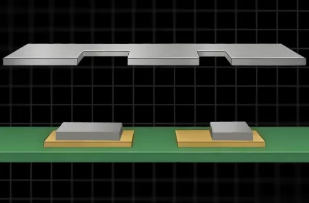
Designers often assume equal copper pads mean equal solder. Stencil reality disagrees. Aperture size, shape, wall quality, area ratio, and print direction all change how much paste leaves the stencil. Two apertures drawn at the same nominal size can still print differently if one sits next to a large opening, a keep-out, or a stepped-stencil transition.
Print variation is normal. Squeegee pressure, stencil cleanliness, pad surface (ENIG vs HASL), and paste slump before reflow all move volume from pad to pad. Industry practice treats a paste-volume mismatch above roughly 15% on a chip pair as a tombstone risk. For 0201 and 01005, the tolerance is tighter because the absolute deposit is already small.
Stencil design is the controllable half of that problem. Use matched apertures for each chip pair. Avoid oversizing one opening to "help wetting" on a plane-connected pad—that extra volume increases pull on the already-faster or already-heavier side. Home-plate or reduced-inner-edge apertures can cut paste behind the termination, which reduces the lifting moment. Specify stencil thickness for the smallest parts on the board; a 5–6 mil foil that works for 0603 can dump too much paste on 0201.
If the board mixes fine-pitch ICs and chip passives, a stepped stencil or a dedicated SMT stencil quote review is cheaper than discovering volume imbalance at first article. Paste inspection (SPI) then confirms that the print you designed is the print you got.
Identical Pads Can Still Heat and Wet Differently
The second driver in the video is copper. Two pads can share the same soldermask opening and still connect to very different thermal masses. One pad leaves on a 0.15 mm signal trace. The other pours straight into a ground plane, a wide power neck, or a via farm. During reflow the plane-connected pad dumps heat into copper. The trace-connected pad reaches liquidus first and pulls.
The temperature gap does not need to be large. Small case sizes fail at a few degrees of pad-to-pad delta. That is why "the pads look the same in the 2D view" is not a thermal argument. You have to look at the copper attached to each pad: trace width, plane ties, thermal reliefs, and nearby vias.
Thermal reliefs exist to solve this. Four spoke ties from a pad into a plane slow heat flow so both ends of the chip heat on a similar clock. Skipping reliefs on one side only—"this pad is GND, pour it solid"—is a common NPI failure on decoupling capacitors sitting on a ground pour. Via-in-pad without fill under one termination is another hidden heat sink.
Soldermask definition can create a second, quieter imbalance. A solder-mask-defined pad and a copper-defined pad on the same part expose different metal area. Wetting force follows exposed copper, not the courtyard outline. Keep both lands the same definition style unless the footprint standard requires otherwise.
Pre-Release DFM Checks That Stop Tombstoning Before the Oven
The video's release checklist is the right sequence: pad symmetry, copper connections, stencil apertures, paste volume, placement accuracy—then reflow. Do this on the layout and the stencil gerber, not after the first panel comes back with upright 0402s.
Start with the footprint. Both lands of a chip pair should match length, width, spacing, and soldermask expansion. Follow the component vendor land pattern or IPC-7351 geometry; do not stretch one pad to reach a via or to clear a courtyard conflict. If the library was built years ago for hand solder, replace it before a dense SMT run.
Then inspect copper attached to each land. If one pad ties to a plane, give the other pad a comparable thermal path or add thermal reliefs on the plane side. Mirror vias. Do not drop a thermal via under only one termination. On HDI PCB and 4 layer PCB designs, plane proximity changes by layer—check the stack-up, not only the top copper.
Stencil and print come next. Match apertures. Confirm area ratio for the smallest chips. Call out SPI limits for chip pairs. If the assembler owns stencil design, send a note on which reference designators are 0201/0402 and which pads sit on planes. That single note prevents a generic 1:1 aperture set from fighting your copper.
Placement last. Require the pick-and-place program to center the body on both lands, not to favor the silk outline. Tombstoning after a nozzle or vision change is often a 50 µm shift, not a new layout. For PCB prototype builds, run a short reflow sample on the real stack-up and the real paste before freezing the stencil.
Rework is not a process plan. Standing a part back down changes the joint twice and still leaves the imbalance for the next board. Fix the pair of pads, the aperture, or the placement offset.
| Risk factor | What actually goes wrong | DFM / process control |
|---|---|---|
| Pad geometry | One land longer, wider, or farther from the body; spacing too open | Matched lands per vendor/IPC-7351; correct gap so both terminations sit on paste |
| Copper / thermal mass | One pad on a plane or wide pour, the other on a thin trace | Thermal reliefs, mirrored vias, comparable neck-downs |
| Stencil / paste volume | Unequal apertures, poor release, >~15% volume delta | Matched apertures, SPI on chip pairs, thickness sized to smallest parts |
| Placement | Body shifted toward one pad | Centering spec in the PnP program; first-article X-ray/AOI on 0201/0402 |
| Reflow | One side reaches liquidus first (ramp too steep, local heat sink) | Soak profile, nitrogen optional, do not use profile as a substitute for layout balance |
Package Size, Copper Mass, and Application Risk
Tombstoning risk scales with mass, termination area, and how aggressive the copper is around the part. 01005 and 0201 fail first. 0402 is the volume workhorse that still produces most factory escapes. 0603 is usually stable unless one pad is dumped into heavy copper. Heavy copper PCB and aluminum PCB constructions change the heat clock again: metal-core and thick-copper boards pull heat out of pads faster, so thermal relief and profile matter more, not less.
Application sets the cost of a miss. A tombstoned pull-up on a consumer electronics PCB may be a functional fail found in test. The same open on an industrial control PCB I/O filter or an aerospace PCB sense network can be a latent field failure. Procurement teams should treat tombstone rate as an assembly-capability metric: ask for SPI data on small chips, AOI escape history, and whether DFM includes thermal-symmetry review—not only minimum pad size.
When you request a PCB assembly quote, include the smallest case size, surface finish, and whether chip parts sit on planes. Those three facts change stencil design and first-article risk more than board outline or color. Prevent tombstoning in design and print. Do not wait for the oven to reveal it.
FAQ
Q1: Does matching pad size in the CAD library prevent tombstoning?
A1: No. Equal pad outlines are necessary, not sufficient. Stencil apertures can still print unequal paste, and the copper connected to each pad can still heat the two ends on different clocks. Review the pair of pads plus attached copper and the stencil, not only the footprint dimensions.
Q2: When does paste-volume mismatch become a tombstone risk?
A2: A practical factory threshold is about 15% volume difference between the two pads of a chip component. Below 0402, the same percentage is a smaller absolute deposit, so SPI limits should be tighter. Oversizing one aperture to "help" a plane-connected pad often increases lift instead of fixing wetting.
Q3: Why do 0201 and 0402 capacitors tombstone more than larger passives?
A3: Lower mass, smaller termination area, and tighter process windows. Capacitor terminations also wrap more of the body than many chip resistors, so molten solder has more surface to grab. Heavy-copper or plane-tied pads make the imbalance worse on those small case sizes.
Q4: Can a reflow-profile change replace a layout fix?
A4: A longer soak and a controlled ramp can reduce time-to-liquidus mismatch, and nitrogen can improve wetting. Neither corrects a pad that is a heat sink or a stencil that prints 30% more paste on one side. Use profile as a process assist after DFM, not as the primary fix.
Q5: What should be on an SMT DFM package so the assembler can prevent tombstoning?
A5: Gerbers and centroid, smallest case size list, note which chip pads tie to planes, surface finish, stencil thickness/aperture rules, and SPI/AOI expectations. If you already have a preferred land pattern, send it. Ambiguous libraries plus undocumented plane ties are the usual first-article surprises.
You're looking at a tombstone—but not the kind you think.
This one is sitting on a PCB.
It's called tombstoning.
It hits chip resistors, capacitors, and small inductors.
One end solders down, the other lifts and stands completely upright.
The real cause is unbalanced solder forces.
When one pad's solder melts earlier, has different volume, or faces different heat, surface tension pulls harder and tips the part.
Two common drivers: solder paste and copper.
Identical pad size does not mean identical paste volume—stencil and print variation create imbalance.
Two pads can look the same yet connect to different copper areas, so they heat and wet differently.
Before release, check pad symmetry, copper connections, stencil apertures, paste volume, and placement accuracy.
Prevent tombstoning before the board reaches the oven.





