










ESP32 Fingerprint Attendance PCB: Reliable 2-Layer Design Ends Breadboard Failures
Key Moment
- 0:00 Introduction & Project Overview
- 1:45 AIVON PCB Sponsorship
- 2:10 Components Required
- 2:40 R503 Fingerprint Sensor Explained
- 3:39 Schematic Design
- 4:04 PCB Layout & 3D View
- 4:30 Ordering the Custom PCB
- 4:55 Assembling the Hardware
- 5:32 Coding & Libraries
- 6:38 Uploading the Code
- 7:03 System Initialization & Scan Mode
- 7:29 Web Dashboard Overview
- 7:54 User Registration & Enrollment
- 8:42 Entry / Exit Tracking & Live Feed
- 9:32 CSV Export & Outro
Project Background
Biometric attendance systems for schools, laboratories and small offices demand more than a working demo. They require consistent fingerprint matching, instant status feedback and a self-hosted dashboard that never incurs cloud fees. Most maker projects begin on a breadboard with an ESP32, an R503 capacitive fingerprint sensor and a 0.96-inch OLED. On the breadboard the system appears functional—until the first real enrollment session. Power spikes during image capture pull the ESP32 into brownout, long jumper wires create intermittent UART contacts, and the R503's strict 50 mV peak-to-peak ripple limit is routinely violated. The result is unreliable scans, lost templates and a prototype that never leaves the workbench.
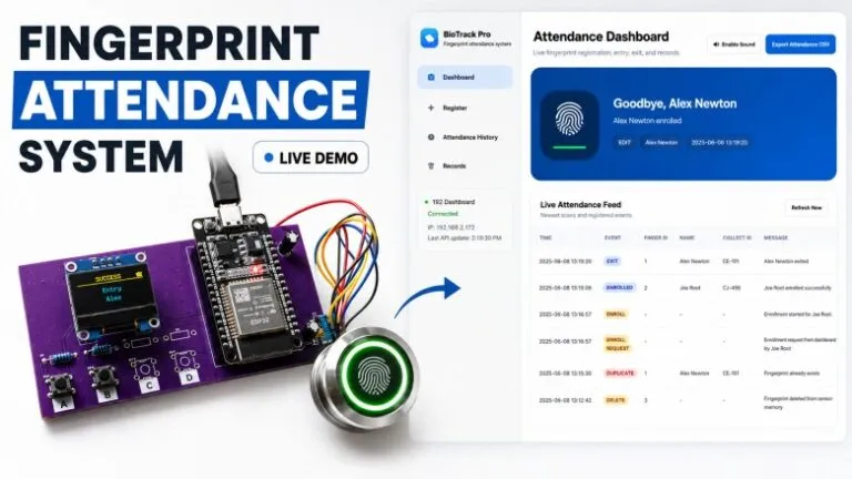
The creator of this project set out to solve exactly that problem. The goal was a practical, field-ready unit: register a user once with name, college ID, department and role; scan for entry or exit; display the result instantly on the OLED; and update a responsive, self-hosted web dashboard in real time. Live attendance feed, duplicate warnings, delete logs and one-click CSV export were all required—without external servers. Moving from breadboard chaos to a compact custom 2-layer FR4 PCB was the decisive step that turned an intermittent experiment into a system ready for daily classroom or lab use.
What This Video Covers
The video walks through every stage of the transformation. It begins with the functional requirements and the limitations of the breadboard prototype, then moves to schematic capture in EasyEDA and the conversion to a double-sided layout optimized for hand assembly. Key hardware moments include the placement of female headers for the ESP32, OLED and R503 modules, the precise positioning of local decoupling capacitors, and the routing of short UART (GPIO16/17) and I2C (GPIO21/22) traces. Firmware integration is shown in detail: Wi-Fi connection, Adafruit Fingerprint library operation, OLED status animations and the complete responsive dashboard stored in PROGMEM. Live enrollment, 1:1 verification, 1:N search across 200 templates, real-time dashboard updates and CSV export are all demonstrated. The video closes with the assembled unit operating cleanly—power stable, mechanical connections solid and the entire system looking finished enough to hand to a lab technician without explanation.
Project Highlights and Key Features
- R503 sensor supporting both 1:1 verification and 1:N search across 200 templates with a straightforward two-scan enrollment process.
- Instant OLED feedback showing the user's first name and exact entry or exit timestamp.
- Fully self-hosted, responsive web dashboard accessible via the ESP32's local IP—user list with finger ID and department, scrolling attendance history, enrollment status, duplicate warnings, delete logs and one-click CSV export.
- Modular female-header architecture allowing the ESP32, OLED or fingerprint module to be swapped without desoldering.
- Optimized 2-layer FR-4 stack-up (1.6 mm, 1 oz copper, lead-free HASL) with continuous ground pour on both sides and selective via tenting.
- Local decoupling (10 µF electrolytic + 0.1 µF ceramic) placed within a few millimetres of the power pins to keep ripple under the R503's 50 mV limit.
- Through-hole dominant design that keeps hand assembly straightforward while still delivering a professional, production-ready appearance.
- Clean mechanical interfaces that eliminate the intermittent contacts and stress previously caused by long jumper wires.
Challenges Encountered During Development
Power integrity was the first and most persistent obstacle. The R503 datasheet is unambiguous: ripple must remain below 50 mV peak-to-peak or the image sensor produces unreliable data. On the breadboard, the current spike during fingerprint capture frequently dragged the 3.3 V rail low enough to reset the ESP32 or scramble the UART link. Long, loose jumper wires to the sensor's 6-pin connector compounded the problem with intermittent contacts and mechanical stress.
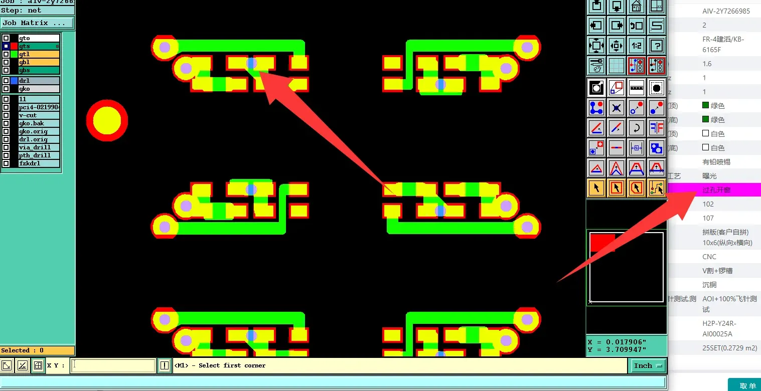
A second class of issues appeared at the manufacturing interface. System parameters called for open vias while the Gerber solder-mask layers showed partial tenting.
Large non-plated holes and connection tabs without stamp holes risked edge quality and dimensional accuracy during depanelisation.
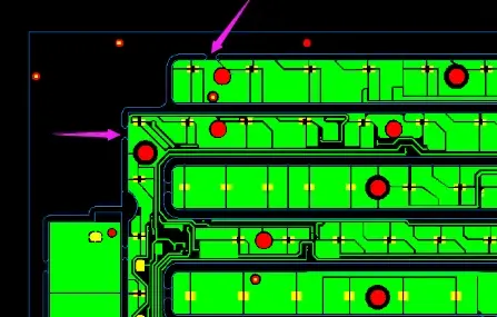
These were ordinary DFM realities rather than exotic failures, yet they are exactly the points at which many biometric prototypes remain stuck in "almost working" status. Without short power and ground runs, continuous ground pours, correctly placed capacitors and clear fab notes on via treatment and hole processing, the board would never have delivered the clean scans and mechanical reliability required for daily deployment.
How AIVON PCB Helps
Once the Gerbers were finalized, the creator ordered a small panel from AIVON. The boards arrived in three days—clean edges, sharp silkscreen, solid plating through every hole. That rapid turnaround kept project momentum high and allowed immediate focus on firmware.
AIVON's engineering support proved equally valuable. When the selective-tenting intent needed clarification, CAM feedback and quick file regeneration ensured the boards passed HASL without solder wicking or probe problems. On parallel 2-layer work, oversized holes were converted to precision routing and standard stamp-hole patterns were added so depanelisation stayed clean and dimensions remained inside Class 2 limits. Clear communication and sensible process choices turned potential holds into on-time delivery.
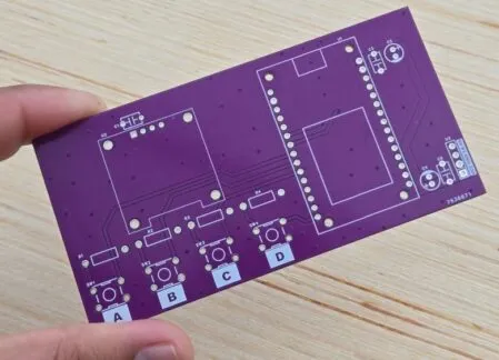
The finished AIVON 2-layer boards eliminated the noise, intermittents and mechanical fragility that normally keep biometric prototypes in demo mode. Power stability improved immediately: fingerprint captures no longer triggered resets. The OLED and web dashboard stayed perfectly synchronized. Modular headers made iterative testing simple—pull a module, swap it, re-test, continue. The same practical DFM discipline that solved via coverage, ground continuity and local decoupling on this attendance board is available to every engineer who needs a reliable 2-layer or multi-layer solution for ESP32, fingerprint or other IoT biometric designs. AIVON combines fast-turn prototyping, expert DFM analysis, high-quality fabrication and reliable delivery into a single, transparent process that moves projects from breadboard to deployable hardware without unnecessary iteration.
Conclusion
A clear functional goal, careful layout decisions and boards that arrived clean and on time transformed a promising biometric demo into a system ready for classroom or laboratory use. The custom 2-layer PCB did more than replace wires—it removed the power spikes, contact resistance and mechanical weakness that had previously kept the design from being dependable day after day.
Anyone still wrestling with a similar ESP32 fingerprint, RFID or IoT attendance project on a breadboard can take the same step. The next move is not more code; it is a board that stops fighting the sensors. A well-executed 2-layer design paired with a manufacturing partner who answers the real engineering questions can take the same idea from "almost" to "ready."
FAQ
Q1: Why is a custom 2-layer PCB essential for an R503-based ESP32 fingerprint attendance system?
A1: Breadboards introduce contact resistance, long traces and noise that violate the R503’s 50 mV ripple limit and cause ESP32 brownouts. A properly designed 2-layer board with short power/ground runs, continuous ground pour and local decoupling delivers the stable power and signal integrity required for reliable daily scans.
Q2: What board stack-up and surface finish work best for this class of biometric prototype?
A2: Standard 2-layer FR-4, 1.6 mm thick, 1 oz copper on both sides with lead-free HASL is sufficient. Continuous ground pours on both sides and selective via tenting further isolate noise while keeping hand assembly straightforward.
Q3: How does selective via tenting improve performance on a fingerprint attendance PCB?
A3: Selective tenting protects vias near noisy digital or power nets, reducing the chance of noise coupling into the R503 or OLED paths, while leaving other vias open for probing or soldering. Clear fab notes ensure the manufacturer applies the correct treatment.
Q4: What decoupling strategy prevents ESP32 resets during fingerprint capture?
A4: Place a 10 µF electrolytic and a 0.1 µF ceramic capacitor within 5 mm of the power pins of both the ESP32 and the R503. Combined with short, wide power traces and a solid ground plane, this keeps the 3.3 V rail stiff under the sensor’s capture current spikes.
Q5: Are female headers suitable for a board that may later move into light production?
A5: Yes for prototypes and small runs—they enable rapid module swaps and field service. Once the design is frozen, the same footprint can transition to direct solder or board-to-board connectors without a full redesign.
Hi everyone, it's me Ha from How to Electronics. Today I am going to show you how I designed an ESP32-based fingerprint biometric attendance system with a professional web dashboard.
This system can register users, scan fingerprints, mark entry and exit attendance, and display all records in real time. For this project, I use an ESP32 development board as the main controller, an R503 fingerprint sensor for biometric verification, and a 0.96 inch OLED display to show system messages, fingerprint status, username, entry, exit, and registration process.
The ESP32 connects to a Wi-Fi network and hosts a beautifully designed local web dashboard. The dashboard has multiple sections such as dashboard, register, attendance history, and records. The main dashboard shows live fingerprint activity, system status, latest events, and attendance feed in a clean and professional layout. You can export the attendance data as well as later view it in Excel or Google Sheets.
This project is very useful for schools, colleges, offices, labs, and organizations where accurate and secure attendance tracking is required. So, let's find out how we can build this ESP32 fingerprint biometric attendance system. Let's get started.
The PCB used in this project is sponsored by Aivon, a global leader in PCB manufacturing and assembly. Aivon provides high quality PCBs with fast production and delivery times. For new users, there is currently a special campaign that includes free shipping and generous discounts, making PCB prototyping far more affordable. You can get a PCB at $1 and PCBA service as low as $35 only and with free shipping.
Welcome back again. Let's take a look at the components required to build this project. First, we need an ESP32 microcontroller board. Then, a fingerprint sensor. I am using an R503 capacitive fingerprint sensor, a 0.96 inch OLED display, some capacitors of 10 microfarads, and 100 nanofarads. You can buy all of these components easily from anywhere.
Let's have a technical overview of the R503 fingerprint sensor. The R503 is an integrated biometric fingerprint module that contains an optical or capacitive sensing area, a built-in DSP processor, flash memory, and a UART communication interface. It does not send the raw fingerprint image to the ESP32 for matching. Instead, the sensor captures the fingerprint, extracts unique feature points, creates a fingerprint template, and stores this template inside its internal memory. The R503 communicates with the ESP32 using UART serial communication, usually at a 57600 baud rate.
Here is the circuit diagram for this project. The ESP32 is the main controller of the system. It reads fingerprint data from the R503 fingerprint sensor through UART communication. The OLED display is connected to the ESP32 through I2C and is used to show messages. Push buttons are also connected to the ESP32 for manual control functions like enrollment and cancel. But in this project, we are not using the push button functions. Capacitors are added near the power supply lines to improve stability and reduce noise during operation.
After designing the schematic, I converted it into a compact PCB layout. All the components are placed on the front side for easier assembly. The routing is done based on signal requirements and component placement. Here is the 2D view of the board from the front side and also from the back side. Similarly, here is the 3D view of the board. The 3D view looks awesome.
So, the next step is to order the PCB. The Gerber files were generated and uploaded to Aivon. Uploading the Gerber file is simple. Just select the board parameters like material, thickness, solder mask, color, and quantity. And here you can just see the total quote of just $1. And shipping is also free. If you want to order a PCB for just $1, click the first link in the description.
I placed the order and within a few days I received these high quality PCBs. The finish, silk screen and through-hole plating were excellent.
Next, I soldered all of the components for 15 minutes. The assembly was smooth and the board looks professional once completed. For ESP32 and OLED display, I am using a female header. I could insert all components easily here. For the R503 fingerprint sensor, I use wires as the sensor needed to be placed in a particular position.
Now, let's move to the coding part. We will develop a C++ code to interface the R503 fingerprint sensor and OLED display with ESP32 and visualize the fingerprint attendance on a web page.
The code starts by including the required libraries for the project. The Wi-Fi and web server libraries are used to connect the ESP32 to a Wi-Fi network and create a local web dashboard. The Adafruit fingerprint library is used for R503 communication with the ESP32. The Adafruit GFX and Adafruit SSD1306 libraries are used to control the OLED display.
In the Wi-Fi section, the SSID and password are added so the ESP32 can connect to the local network. The main loop continuously reads data from the R503 sensor. These readings are displayed on the OLED screen, printed on the serial monitor, and sent to the web dashboard as JSON data through the API readings route.
Here's the header file for the project. The dashboard.h file contains all of the HTML, CSS, and JavaScript code used to create the live web view.
Once the hardware assembly is complete, it's time to upload the code. In the Arduino IDE, go to tools, board, and select ESP32 dev module. Then choose the correct COM port. Finally, click the upload button. The code will be uploaded to the ESP32 board.
After uploading the code to the ESP32, the device starts initializing all the connected modules. The OLED display first shows the Wi-Fi connection status. Once the ESP32 connects to the local Wi-Fi network, it displays the IP address on the OLED screen. Finally, the system enters scan mode. In this mode, the OLED display displays "Place finger" and waits for a registered fingerprint.
To access the web dashboard, enter the IP address on a web browser. The dashboard page shows the live fingerprint system status, Wi-Fi connection, latest API update time, and live attendance feed. From the left side menu, we can open different sections such as dashboard, register, attendance history, and records.
The register page is used to add student or staff details and start fingerprint enrollment. To register a new fingerprint here, enter the user details such as name, college ID, role and department. Then click the start registration button.
After starting the registration, the dashboard shows an enrollment started popup and the OLED display asks the user to place a finger on the R503 fingerprint sensor. The sensor first captures the fingerprint image, then asks the user to remove the finger and place the same finger again for the second scan. Once both scans are matched successfully, the fingerprint template is saved in the R503 sensor memory and the user details are stored in the ESP32.
If the same registered finger is scanned again during the registration process, the system detects it as a duplicate fingerprint.
For the first scan, the dashboard displays a welcome popup with the user's name, fingerprint ID, college ID, and department. This means the user has entered and the entry time is saved in the attendance log. When the same user scans again, the system records it as an exit and displays a goodbye or exit logged message on the dashboard.
If an unknown or unregistered finger is scanned, the OLED display shows a try again or search failed message. The dashboard also keeps updating the live attendance feed, attendance history, and student staff records.
The dashboard also provides an export attendance CSV option. This allows the attendance history to be downloaded as a CSV file which can be opened in Excel or Google Sheets for recordkeeping.
That's all from the video part today. All of the detailed written guides related to this project can be found on the website article of how to electronics. You can find the bill of materials, schematic, PCB, Gerber file, source code, program and other instructions here.
I hope you like this video. So, why not drop a like and hit the subscribe button? Finally, thank you so much for watching. See you in the next video.





