During CAM review of a standard 2-layer FR-4 board with customer-supplied panelization, several manufacturing details required clarification before the job could be released. The design included multiple large-diameter holes exceeding 3 mm, connection tabs without stamp holes, and a customer note requesting IPC Class 2 consideration. These points triggered Engineering Questions because they directly affect contour accuracy, depanelization reliability, and tolerance stack-up under our standard process window. Our CAM engineer examined the Gerber and drill data against the fabrication notes and production constraints for a 1.6 mm TG150 board finished with lead-free HASL. The following case reconstructs the actual decision path that converted an ambiguous data package into a manufacturable release.
Order Overview: 2-Layer Panelized Board with Mechanical Forming
The order called for a 2-layer FR-4 board ( #FR4-20260530-026 ) (KB-6165F equivalent, TG150) measuring 169 mm × 411.67 mm, thickness 1.6 mm, with 1 oz copper on both sides. Surface finish was lead-free HASL, solder mask cold white on both sides, and silkscreen black on both sides. Minimum finished hole size was specified at 0.4 mm, line width/space 10 mil, and 100 % flying-probe testing was required. Quantity was 60 pieces delivered as 15 customer-defined panels in a 1 × 4 array, separated by V-groove with zero process edge and zero V-groove spacing tolerance listed. Forming method was mechanical, via tenting applied, no half-holes, no impedance control, and no resin-filled vias. Hole density reached approximately 6700 holes per square meter, routing length totaled 113 mm, and the customer note simply stated "Consider IPC class 2." Production confirmation was already marked "yes," and the factory number indicated an engineering-file status awaiting final CAM clearance.
Because the panel was customer-supplied and the outline relied on V-groove plus connection tabs, any ambiguity in large-hole treatment or breakaway features would immediately affect both dimensional yield and assembly edge quality. Our engineer therefore opened the data package with particular attention to hole-size distribution and panelization integrity.
Large Hole Precision Routing Decision During CAM Review
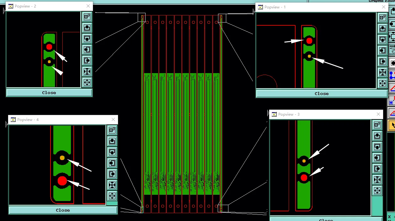
The first critical observation appeared in the drill and outline layers: several non-plated holes exceeded 3 mm in diameter. In standard PCB processing, holes larger than approximately 3 mm are frequently converted from drilling to contour routing when tight positional or diameter tolerance is required, or when the hole edge must meet the same quality as the board outline. Our CAM engineer measured the actual diameters against the tooling capability for a 1.6 mm FR-4 panel and noted that the design provided no explicit call-out distinguishing plated versus non-plated large holes, nor any tolerance table beyond the generic IPC Class 2 request.
If these large holes had been left as conventional drill features, two realistic risks would arise. First, drill bit deflection and spindle run-out on diameters above 3 mm can produce ovality and positional drift that exceed typical Class 2 hole-location allowances. Second, the exit burr and wall roughness after drilling a large hole in 1.6 mm material are often inferior to a properly programmed routing path, increasing the chance of residual copper or resin smear that later affects solderability or mechanical fit. We therefore raised the EQ: "Data contains holes larger than 3 mm; please confirm whether precision routing is required."
After internal discussion, the engineering team recommended converting all non-plated holes above 3 mm to precision contour routing using a compensated routing bit path. This approach keeps the hole center within the same coordinate system as the board outline, improves edge quality, and aligns with the mechanical-forming method already specified for the panel. The customer was asked to confirm the conversion so that the CAM data could be updated before tooling release. Leaving the holes as drilled would have risked scrap for dimensional non-conformance and potential assembly interference, especially given the zero process-edge condition of the panel.
Panelization Tabs Without Stamp Holes: Breakaway Risk Assessment
The second major issue concerned the customer-supplied panelization. Multiple connection tabs were present between the individual boards inside the 1 × 4 array, yet no stamp holes (mouse-bite or stamp-hole features) had been designed. In a V-groove panel with zero process edge, the mechanical integrity of the array during routing, HASL, and shipping depends almost entirely on those tabs. Without stamp holes or controlled breakaway perforations, the tabs remain solid copper-clad FR-4 strips that must later be broken by hand or fixture. Our CAM engineer observed that the tab width and copper coverage were inconsistent across the panel, raising the probability of uneven stress during depanelization.
If production had continued without clarification, two failure modes were realistic. First, excessive force required to snap the solid tabs could induce board warpage or micro-cracks near the V-groove, especially on a 1.6 mm TG150 laminate that has already undergone thermal cycling in HASL. Second, irregular fracture surfaces could leave residual material or exposed copper fibers along the board edge, violating IPC-A-600 Class 2 edge-quality expectations and creating potential shorting risks during subsequent assembly. We therefore issued the EQ: "Multiple connection positions exist in the data, no stamp holes present; please confirm whether they need to be added."
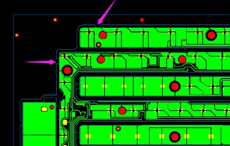
Figure 1: there are many tab routings in this design, but without stamp holes
The engineering recommendation was either to add a standard stamp-hole pattern (typically 0.8–1.0 mm diameter holes on a 1.5–2.0 mm pitch) centered on each tab, or to accept the solid tabs with a written customer waiver that depanelization stress and edge quality remain the customer's responsibility. Because the order already specified mechanical forming and zero process edge, adding stamp holes was the lower-risk path for yield protection. The decision preserved the customer's intended panel outline while reducing the chance of post-depanelization scrap.
Tolerance Interpretation and IPC Class 2 Alignment
A third clarification was required on dimensional tolerances. The customer note simply read "Consider IPC class 2," yet no detailed tolerance table accompanied the fabrication drawing. Our internal process defaults to the factory's standard Class 2 capability window for 2-layer FR-4 work of this complexity. The EQ therefore asked whether the data should follow the factory's conventional tolerances and ignore any conflicting notes: "Could you please confirm whether the material tolerances are being handled according to our standard practice?"
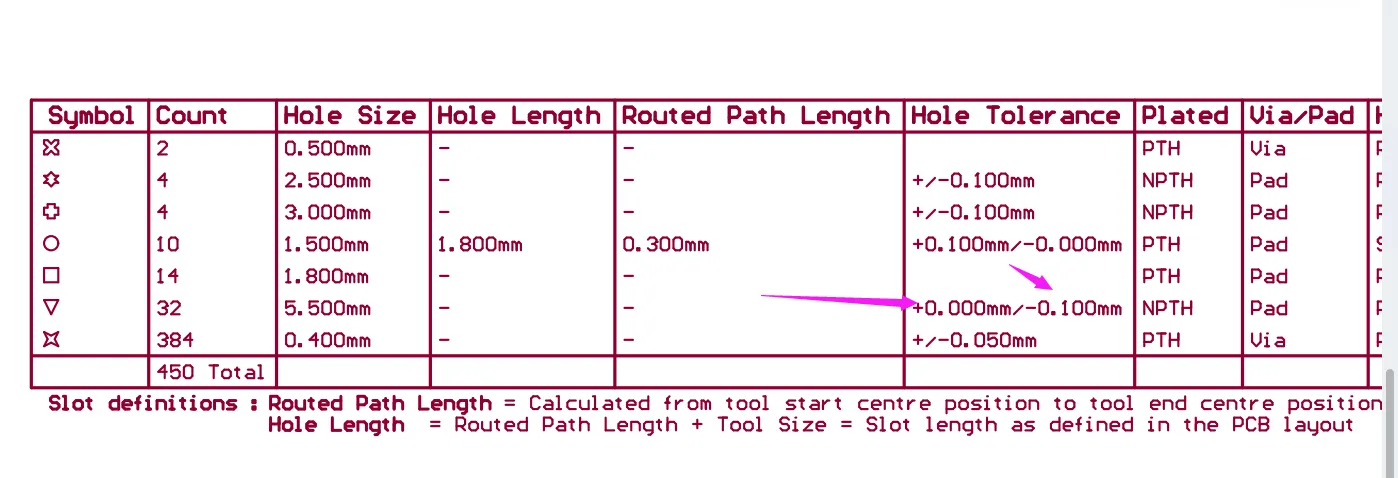
Figure 2: our standard practice
Ignoring this step would have left open the possibility that the customer expected tighter limits on outline, hole position, or V-groove depth than the factory's standard capability. In practice, a mismatch of even 0.1 mm on a large-hole location or tab break-out could trigger dimensional rejection after final inspection. By confirming that the factory standard Class 2 window applied, the CAM team locked the inspection criteria and avoided later dispute. The file-confirmation step that closed the EQ package simply recorded the customer's acceptance of all preceding clarifications.
DFM Risks in Customer-Panelized 2 Layer FR4 Boards
This order illustrated three recurring DFM gaps that frequently appear on 2-layer customer-panelized boards. First, designers often treat all holes the same regardless of diameter; once the diameter crosses the practical drill-to-route threshold (commonly 3 mm), the manufacturing method and resulting edge quality change. Second, connection tabs without stamp holes or mouse bites are common in self-panelized data, yet they shift the depanelization risk entirely onto the assembly process. Third, a generic "IPC Class 2" note without a supporting tolerance table leaves the factory to interpret capability limits, which can differ from the designer's mental model of "Class 2."
If any of these points had been left unresolved, the most probable outcomes would have been: dimensional non-conformance on the large holes, irregular board edges after tab fracture, and potential scrap or rework at the customer's assembly line. Because the panel carried zero process edge and relied on V-groove, there was no secondary routing margin to absorb these defects. The CAM review therefore functioned as the final risk filter before tooling and plating.
| Issue | Risk if Unresolved | Resolution |
|---|---|---|
| Holes Larger Than 3mm | Ovality, positional drift, poor edge quality | Converted to precision contour routing |
| Tabs Without Stamp Holes | Warpage, micro-cracks, irregular edges | Added standard stamp-hole pattern |
| IPC Class 2 Note | Tolerance mismatch and inspection disputes | Confirmed factory standard Class 2 window |
Table 1: Key CAM Issues in This 2 Layer FR4 Panelized Board
How the Engineering Team Resolved the Issues
Our CAM engineer first isolated every hole larger than 3 mm, classified them as non-plated, and prepared a compensated routing path that matched the existing outline coordinate system. The routing compensation accounted for bit diameter and the 1.6 mm material thickness so that finished hole size remained within Class 2 limits. Simultaneously, a standard stamp-hole pattern was proposed for each connection tab; the pattern was sized to maintain panel rigidity through HASL while allowing clean break-out. Both changes were documented in the EQ reply together with a clear statement that factory standard Class 2 tolerances would apply unless the customer supplied a tighter table.
Once the customer confirmed the three points, the production data were updated, the panelization file regenerated, and the job released to the drilling and routing stations. No stack-up change or process-edge addition was required; the existing mechanical-forming flow remained intact. The entire clarification cycle stayed within the two-day lead-time window because the questions were raised early and answered with concrete manufacturing options rather than open-ended requests.
All Engineering Questions were closed with customer confirmation. Large holes above 3 mm were converted to precision contour routing, stamp holes were added to the connection tabs, and dimensional inspection proceeded under the factory's standard IPC Class 2 capability window. The CAM data package was approved, tooling released, and the 15-panel order moved into production without further engineering holds. The finished boards met the dimensional and edge-quality criteria required for subsequent assembly.
Key Takeaways for 2-Layer FR-4 PCB Designers
- When any hole diameter exceeds 3 mm, explicitly state whether the feature should be drilled or precision-routed; silence forces the factory to raise an EQ.
- On customer-supplied panels that use connection tabs, include stamp holes or mouse bites unless a solid-tab waiver is intentional and documented.
- A single-line "IPC Class 2" note is insufficient; attach a tolerance table or accept the factory's published Class 2 window to avoid later dispute.
- Zero process-edge V-groove panels leave no margin for edge defects; any ambiguity in tab design or large-hole treatment directly threatens yield.
- Non-plated large holes and plated vias should be clearly differentiated in the drill attributes so that routing versus drilling decisions can be made without guesswork.
- Provide the fabrication drawing and Gerber files with consistent layer naming and a single source of truth for outline and hole features; conflicting notes trigger automatic EQ holds.
FAQ
Q1: Why do PCB factories ask for confirmation on holes larger than 3 mm?
A1: Diameters above 3 mm often exceed the practical limit for stable drilling accuracy and edge quality. Precision contour routing keeps positional tolerance and wall finish within Class 2 expectations, especially on 1.6 mm FR-4 panels.
Q2: What is the risk of connection tabs without stamp holes on a V-groove panel?
A2: Solid tabs require higher break-out force, which can cause board warpage, micro-cracks near the V-groove, or irregular edge fracture that leaves residual material and fails IPC-A-600 edge criteria.
Q3: Can a factory ignore customer tolerance notes and use its own standard?
A3: Only after explicit customer confirmation. The EQ process documents that the factory's conventional Class 2 window will be applied, preventing later dimensional disputes.
Q4: Does precision routing of large holes affect lead time or cost on a 2-day order?
A4: When the conversion is decided during the initial CAM review, the routing path is programmed once and fits inside the existing mechanical-forming schedule; no extra days are added if the customer responds promptly.
Q5: Why is zero process edge important when evaluating stamp-hole needs?
A5: With no process edge, the panel has no secondary routing margin. Any fracture irregularity on the tabs becomes the final board edge, making stamp holes the primary method for controlled break-out.
Q6: How does IPC Class 2 relate to large-hole and tab decisions?
A6: Class 2 sets the acceptability baseline for hole location, diameter, and edge quality. Converting large holes to precision routing and adding stamp holes are practical steps that keep the finished board inside those limits without requiring tighter customer-specified tolerances.