Introduction
Voltage-controlled oscillators (VCOs) are fundamental building blocks in modern RF and microwave systems, including phase-locked loops (PLLs), frequency synthesizers, radar, and wireless communication equipment. At the heart of most VCO tuning mechanisms lies the varactor diode - a semiconductor device whose capacitance varies with applied reverse bias voltage. Proper varactor diode drive circuit design is essential for achieving linear tuning, low phase noise, wide bandwidth, and high spectral purity.
Varactor Diode Technology and Operating Principles
A varactor (variable capacitor) diode is a PN junction optimized to maximize capacitance variation with reverse voltage. When reverse-biased, the depletion region width changes, altering the junction capacitance. Key parameters include capacitance ratio (Cmax/Cmin), tuning linearity, Q-factor, series resistance (Rs), and breakdown voltage.
Hyperabrupt junction varactors offer more linear tuning characteristics and wider capacitance range compared to abrupt junction devices, making them preferred in many commercial VCO designs despite slightly higher phase noise contribution.
VCO Circuit Architectures and Varactor Integration
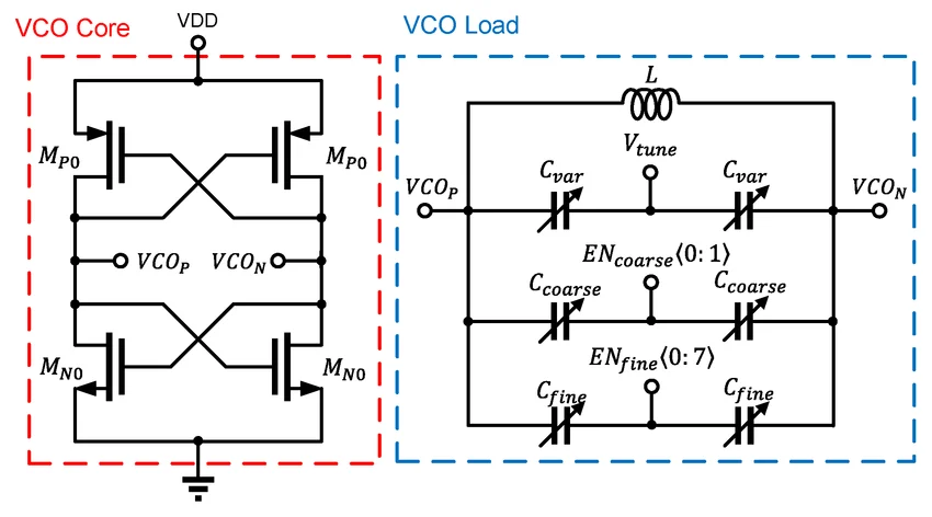
In a typical LC-tank VCO, one or more varactor diodes are connected in parallel with an inductor to form a resonant circuit. The oscillation frequency is determined by the formula: f = 1 / (2pi * sqrt(L * Ctotal)), where Ctotal includes fixed capacitance, parasitic capacitance, and the voltage-variable capacitance of the varactor.
Common configurations include:
- Single varactor tuning
- Back-to-back (anti-series) varactor pairs for improved linearity and reduced distortion
- Switched varactor banks for wideband operation
The varactor drive circuit must provide a clean, low-noise tuning voltage while isolating the RF tank from the control circuitry.
Design Considerations and Engineering Challenges
Successful varactor-driven VCO design involves several critical trade-offs:
Phase Noise Performance
The varactor's series resistance and the tuning voltage supply noise directly contribute to phase noise. Power supply rejection, filtering, and careful grounding are mandatory. Even microvolt-level noise on the tuning line can degrade close-in phase noise significantly.
Tuning Linearity and Kvco
The voltage-to-frequency gain (Kvco) should remain as constant as possible across the tuning range. Non-linearity leads to variable PLL loop dynamics and potential instability. Hyperabrupt varactors help, but compensation circuits or digital pre-distortion are often required.
Control Voltage Range and Linearity
Most varactors operate between 0 V and 20-30 V. The drive circuit must generate a stable, low-noise voltage across this range. Op-amp based active filters or precision DACs followed by low-noise buffers are common solutions.
Thermal Stability
Junction capacitance varies with temperature. High-power VCOs or designs operating over wide temperature ranges require compensation techniques or temperature-controlled environments.
Manufacturing and Reliability Considerations
Varactor diodes are sensitive to parasitic inductance and capacitance. Assembly processes must minimize lead lengths and ensure repeatable solder joint quality. In high-volume production, consistent PCB material properties and controlled impedance become critical for maintaining center frequency and tuning range across units.
Materials, PCB Design, and RF Layout Strategies
PCB design is one of the most influential factors in VCO performance. Key considerations include:
- Controlled Impedance Transmission Lines: Microstrip or coplanar waveguide structures must maintain 50 Ohm impedance with tight tolerance.
- Low Parasitic Layout: The varactor should be placed as close as possible to the resonator inductor. Via placement and ground plane integrity directly affect Q-factor.
- Tuning Voltage Routing: The varactor control line must be heavily filtered and isolated from digital or switching noise. Separate analog ground planes or careful star grounding is often necessary.
- PCB Material Selection: Low-loss dielectric materials (Rogers, Taconic, or high-performance FR-4) are preferred. Consistent dielectric constant (Dk) and low dissipation factor are essential for stable oscillation frequency.
- Thermal Management: In high-power VCOs, thermal vias and copper pours help stabilize device temperature and reduce frequency drift.
Flexible circuits (FPC) are sometimes used in compact or portable designs to connect varactor control signals while minimizing mechanical stress and parasitic effects.
Industry Trends
The demand for wider tuning bandwidth, lower phase noise, and smaller form factors continues to push varactor and VCO technology. Modern designs increasingly combine varactors with MEMS capacitors or switched capacitor banks. At the same time, PCB fabricators are being asked to deliver tighter tolerances on trace geometry, dielectric thickness, and material consistency to support millimeter-wave and 5G applications.
How PCB Technologies Enable High-Performance VCO Systems
Reliable varactor-driven VCO performance depends heavily on the supporting PCB platform. PCB fabrication must deliver precise control over trace width, spacing, copper thickness, and dielectric properties to maintain consistent impedance and minimize losses in the resonant tank. High-frequency laminates with stable Dk across temperature and frequency are often required.
From a manufacturing standpoint, accurate registration, smooth copper foil, and repeatable solder mask application directly influence parasitic capacitance and Q-factor. Thermal solutions such as dense via arrays and controlled copper balancing help reduce frequency drift. These engineering and production factors determine whether a VCO meets critical specifications for phase noise, tuning range, and long-term stability in demanding RF and microwave systems.
Frequently Asked Questions
Q1: What is the main advantage of hyperabrupt varactor diodes in VCOs?
A1: They provide more linear frequency tuning and a wider capacitance range, simplifying PLL loop filter design and improving overall system stability.
Q2: Why is low-noise design critical on the varactor tuning line?
A2: Noise on the tuning voltage is directly modulated onto the VCO output as phase noise. Even small voltage fluctuations can significantly degrade signal quality in communications and radar systems.
Q3: What PCB material properties matter most for high-performance VCO circuits?
A3: Low dielectric loss (Df), stable dielectric constant (Dk) over temperature and frequency, consistent thickness tolerance, and smooth copper surface are essential for maintaining high Q and frequency stability.