Introduction
Custom audio filters play a critical role in modern audio systems, enabling precise frequency shaping for high-fidelity sound reproduction. In PCB design, integrating these filters directly onto the board ensures compact layouts while maintaining signal integrity essential for applications like equalizers, crossovers, and noise reduction circuits. Engineers often turn to audio filter design PCB techniques to achieve low distortion and optimal dynamic range in professional audio equipment, consumer devices, and measurement systems. Active filter circuits audio, in particular, offer advantages over passive designs by providing gain buffering and sharper roll-off characteristics without inductors. This tutorial provides a structured approach to Butterworth filter implementation PCB, audio equalization techniques PCB, and low-noise amplifier design audio, drawing on established engineering principles. By following these steps, designers can create reliable circuits that meet performance demands in real-world deployments.
Audio applications demand filters that preserve phase linearity and minimize group delay variations, making custom PCB implementations indispensable. Whether attenuating rumble below 20 Hz or rolling off ultrasonics above 20 kHz, these designs must contend with PCB parasitics like stray capacitance and inductive coupling. The process begins with topology selection and ends with layout optimization for minimal noise pickup. This guide equips electric engineers with practical strategies to navigate these challenges effectively.
Understanding Audio Filters and Their Importance on PCBs
Audio filters classify into low-pass, high-pass, band-pass, and band-stop types, each tailored to specific frequency control needs. Low-pass filters remove high-frequency noise, while high-pass variants eliminate subsonic content that could damage speakers. In PCB contexts, active implementations using operational amplifiers dominate due to their tunability and independence from load impedance. These circuits excel in audio equalization techniques PCB, where multiple stages adjust gain across octaves for tonal balance. Custom designs outperform generic modules by allowing integration with amplifiers and ADCs on the same board.
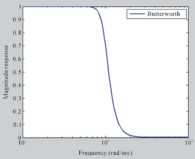
The relevance stems from audio's sensitivity to noise and distortion; even microvolt-level interference becomes audible. PCB-mounted filters reduce interconnection lengths, cutting susceptibility to electromagnetic interference. Butterworth filters stand out for their maximally flat passband response, ideal for transparent audio processing without ripple. Engineers must consider power supply rejection and thermal stability during design. Standards like IPC-2221C guide trace routing and spacing to prevent crosstalk in dense layouts.
Passive filters suffice for simple attenuation but lack the precision of active topologies. Active filter circuits audio enable higher-order responses through cascading, achieving steeper slopes like 24 dB/octave for subwoofer crossovers. PCB realization introduces layout sensitivities, such as feedback path impedance mismatches causing peaking. Addressing these ensures phase-coherent multichannel systems.
Core Technical Principles of Active Audio Filters
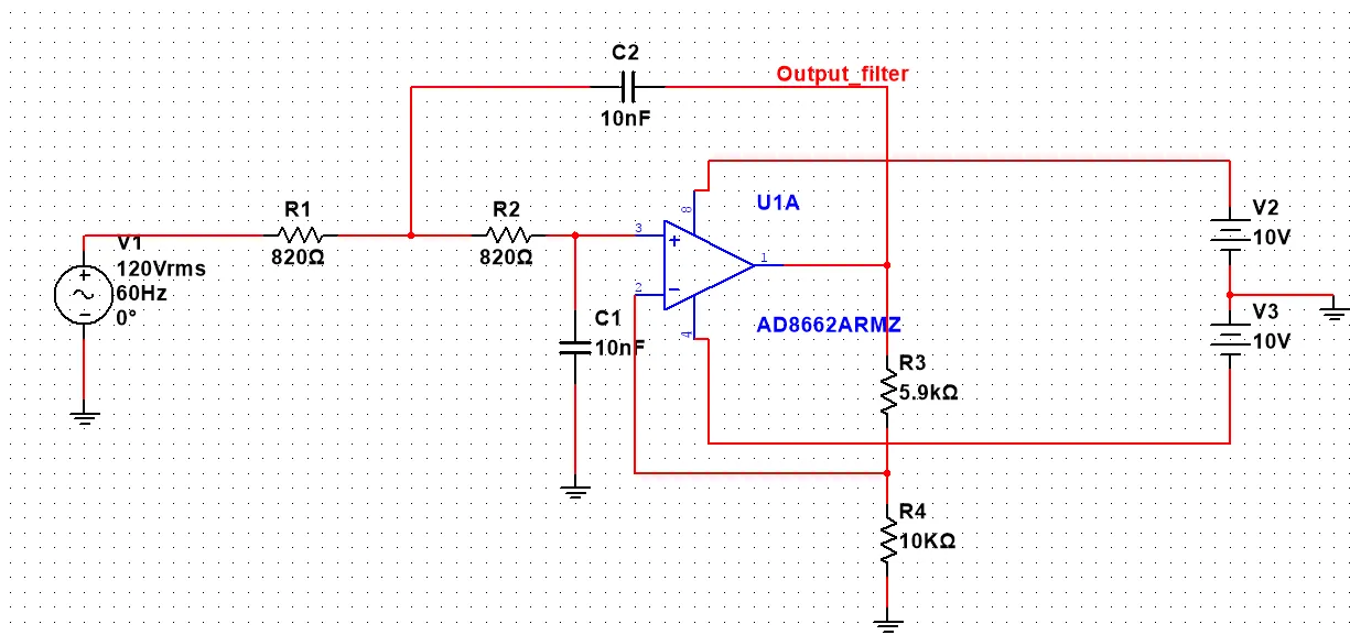
Active filters rely on op-amps configured in feedback loops with RC networks to define poles and zeros. The Sallen-Key topology proves popular for second-order sections due to its simplicity and low component count. For a low-pass stage, the transfer function approximates H(s) = 1 / (1 + s/Qω0 + (s/ω0)^2), where ω0 sets cutoff and Q controls damping. Butterworth filter implementation PCB targets Q = 0.707 per stage for flat magnitude response. Higher orders require multiple unity-gain stages to avoid op-amp overload.
Noise performance hinges on resistor values; lower resistances reduce thermal noise but demand larger capacitors. Op-amp selection prioritizes low voltage noise density, high power supply rejection ratio, and sufficient bandwidth beyond 20 kHz. In cascaded designs, sequence high-Q stages first to attenuate their noise contribution in subsequent sections. PCB parasitics shift pole locations, necessitating simulation validation before layout.
Audio equalization techniques PCB often employ biquad filters, combining notch and peaking responses for parametric control. These allow boost or cut at center frequencies with adjustable bandwidth. Gain staging prevents clipping while maintaining headroom. Grounding schemes profoundly impact common-mode rejection.
Step-by-Step Guide to Audio Filter Design on PCBs
Step 1: Define Specifications and Select Topology
Begin by specifying cutoff frequency, order, ripple tolerance, and input/output levels. For a 1 kHz low-pass Butterworth, a fourth-order design yields -3 dB at cutoff with 24 dB/octave roll-off. Choose active topology based on unity-gain stability needs; multiple-feedback suits voltage-controlled applications. Calculate component values using normalized tables scaled to desired frequency. Precision of 1% for resistors and NP0/C0G ceramics for capacitors ensures Q stability.
Document phase and gain margins early. Consider supply voltage; bipolar ±15 V supports dynamic range exceeding 100 dB.
Step 2: Component Selection and Schematic Development
Select low-noise op-amps with input noise below 10 nV/√Hz for audio bands. Resistor values around 10 kΩ balance noise and capacitor practicality. Simulate the schematic to verify frequency response and transient behavior. Add buffers if driving low-impedance loads. Include DC blocking capacitors to prevent offsets.
For Butterworth filter implementation PCB, denormalize prototype values: C = 1/(2πfR). Verify unity gain at DC for integrators.
Step 3: PCB Layout for Low-Noise Performance
Layout profoundly affects low-noise amplifier design audio integrated with filters. Employ a solid ground plane on the bottom layer, splitting analog sections if mixed-signal. Route signal traces over ground, minimizing loop areas for magnetic coupling rejection. Place decoupling capacitors—0.1 μF ceramic plus 10 μF electrolytic—within 5 mm of each op-amp power pin. Follow IPC-2221C for minimum trace widths and clearances to handle currents without voltage drops. Refer to our guide on high-frequency PCB assembly for additional signal integrity tips in audio circuits.
Star-ground sensitive nodes to a single point, avoiding loops that induce hum at 50/60 Hz. Keep feedback traces short and shielded under ground pours. Separate power routing from signals.
Orient components to shorten high-impedance paths. Use via stitching along ground boundaries for low-inductance returns.
Step 4: Power Supply and Decoupling Optimization
Dedicated low-noise LDO regulators or linear supplies for analog rails minimize ripple. Add LC post-filters or ferrite beads for additional attenuation. Use Kelvin sensing for remote regulation. Stage decoupling capacitors (0.01 µF, 0.1 µF, 1–10 µF, 100 µF) for broadband performance from kHz to MHz. Follow IPC-7351C for land patterns to ensure reliable solder joints and thermal performance. Clean power is essential—power supply noise directly degrades the noise floor of active filter circuits audio.
Step 5: Verification, Prototyping, and Iteration
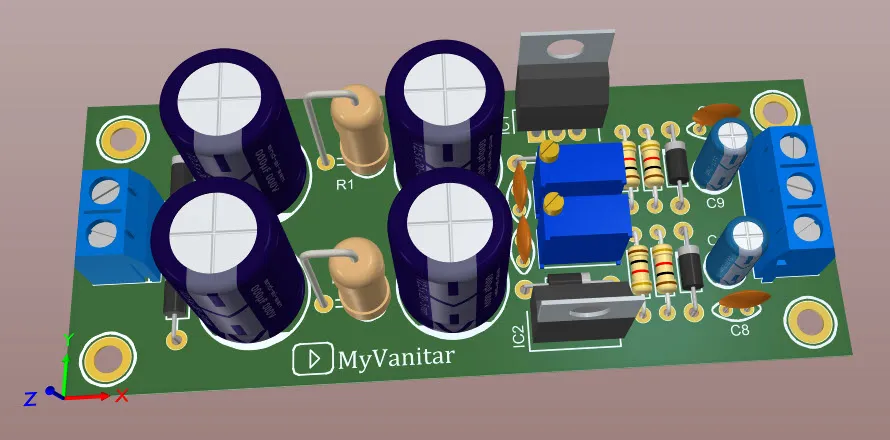
Fabricate prototypes on FR-4 (or lower-loss dielectric for high-precision work), preferably 2- or 4-layer boards. Measure frequency response using a network analyzer or audio analyzer (e.g., swept sine for magnitude/phase, THD+N vs. frequency). Use an oscilloscope to examine square-wave response for ringing (indicating marginal stability) and FFT mode to identify discrete spurs or noise floor. Compare simulated vs. measured Bode plots; adjust for parasitic-induced peaking by tweaking capacitors or adding compensation.
Iterate layout if crosstalk, excessive noise, or thermal drift appears. Assembly per IPC-A-610 standards ensures quality. Thorough measurement validates that Butterworth filter implementation PCB meets specifications for cutoff, roll-off, and dynamic range.
Advanced Techniques: Equalization and Amplification Integration
Audio equalization techniques PCB leverage state-variable filters for simultaneous low-pass, high-pass, and band-pass outputs. Cascade with variable gain stages for shelving or peaking. Low-noise amplifier design audio precedes filters, using instrumentation topology for common-mode rejection. Matched source impedances cancel resistor noise.
Guard traces around inputs shield electrostatic coupling. Multi-layer boards with dedicated planes excel here. For best results, pair your filter design with proven low-noise audio amplifier PCBs techniques.
Simulation and Prototyping Tools for Audio Filters
Simulation prevents costly respins. LTspice remains the gold standard for audio work due to its speed, extensive audio-grade op-amp models, built-in noise analysis, and distortion simulation. KiCad with integrated ngspice offers a seamless open-source workflow from schematic simulation to PCB layout, supporting AC sweeps, transient analysis, and custom models.
Other valuable tools include Altium Designer's integrated SPICE, Texas Instruments FilterLab or TINA-TI for rapid filter synthesis, and MATLAB/Simulink for advanced behavioral modeling. For measurement validation, combine bench instruments with software such as REW (Room EQ Wizard) or ARTA.
For physical prototyping, begin with breadboarding for quick verification, then move to fabricated boards from professional services. KiCad exports Gerbers compatible with most manufacturers. These tools, widely used by competitors, enable accurate prediction of real-world performance before committing to production.
Troubleshooting Common Issues in Audio Filter PCBs
Oscillations arise from phase margin erosion via capacitive loading; add series resistors at outputs. Hum indicates ground loops—lift digital grounds via 10 Ω resistors. Component tolerances shift cutoffs; trim with potentiometers during bench tuning. Excessive noise points to poor decoupling—audit cap placements.
Hum or buzz at 50/60 Hz and harmonics usually indicates ground loops. Use the oscilloscope in AC-coupled FFT mode to pinpoint frequencies, then lift grounds selectively (e.g., via 10 Ω resistor) or enforce strict star grounding. Component tolerances can shift cutoffs—measure the actual –3 dB point and trim with parallel capacitors or potentiometers during calibration.
Excessive noise suggests poor decoupling, high-value resistors, or suboptimal op-amps. Audit capacitor placement and measure the noise floor with a spectrum analyzer. Peaking in the passband may require layout revisions or tighter-tolerance parts. Thermal drift is mitigated with C0G capacitors. EMI pickup benefits from ferrite beads on inputs and shielded cabling. Systematic scoping and iterative measurement typically resolve these issues quickly.
Case Study: Building a Practical Audio Crossover on PCB
A practical example is a fourth-order (24 dB/octave) Butterworth low-pass filter for an active subwoofer crossover at 80 Hz, cascaded with a matching high-pass section for the main speakers. Two Sallen-Key stages per filter path were used with Q values of approximately 0.541 and 1.307.
Component values were scaled from normalized tables (resistors in 10–22 kΩ range, capacitors from 47 nF to 0.47 µF for the low frequencies). LTspice simulation predicted –3 dB at 80 Hz, smooth roll-off, and noise floor below –110 dBu. The PCB layout featured a dedicated ground plane, star grounding for all analog returns, extensive decoupling, and physical separation between low-pass and high-pass sections to minimize crosstalk.
Prototypes fabricated and assembled showed excellent correlation with simulation: measured roll-off matched within 0.5 dB, THD remained below 0.005% at nominal levels, and the integrated low-noise input stage kept the overall noise floor suitably low for hi-fi applications. Minor layout iteration reduced a small 120 Hz spur caused by power supply routing. This case study demonstrates that careful audio filter design PCB practices, combined with simulation and star-grounding techniques, deliver professional-grade performance in a compact, cost-effective format.
Conclusion
Designing custom filters for audio on PCBs demands meticulous attention from specification to layout, ensuring low distortion and robust performance. Key steps—topology selection, precise component choice, and noise-optimized routing—unlock high-fidelity results. Integrating active filter circuits audio with equalization and amplification elevates system quality. Adhering to standards like IPC-2221C guarantees manufacturability. Engineers can confidently prototype these designs for diverse applications.
FAQs
Q1: What are the basics of audio filter design PCB for electric engineers?
A1: Audio filter design PCB involves selecting active topologies like Sallen-Key for precise frequency control. Define cutoffs and orders first, then size RC components for desired response. Layout emphasizes ground planes and short feedback paths to minimize noise. Simulation verifies performance before fabrication, ensuring compliance with signal integrity needs.
Q2: How does Butterworth filter implementation PCB improve audio quality?
A2: Butterworth filter implementation PCB delivers flat passband response ideal for undistorted audio. Cascade second-order stages with Q = 0.707 for higher orders. PCB layout must mitigate parasitics to preserve roll-off. This approach suits crossovers and anti-aliasing, maintaining phase linearity across the audible spectrum.
Q3: What are key audio equalization techniques PCB?
A3: Audio equalization techniques PCB use biquad or state-variable filters for boost/cut at specific frequencies. Parametric designs adjust Q and gain per band. Integrate with low-noise amps on split planes to reject interference. Cascading enables graphic EQ emulation with minimal phase shift.
Q4: Why focus on low-noise amplifier design audio in filter PCBs?
A4: Low-noise amplifier design audio preconditions signals for filters, maximizing dynamic range. Use low-eNoise op-amps and star grounding to suppress hum. Decouple aggressively and route powers separately. This integration prevents noise floor elevation, critical for hi-fi and professional recording applications.
References
IPC-2221C — Generic Standard on Printed Board Design. IPC, 2023
IPC-7351C — Generic Requirements for Surface Mount Design and Land Pattern Standard. IPC, 2014
IPC-A-610H — Acceptability of Electronic Assemblies. IPC, 2019


