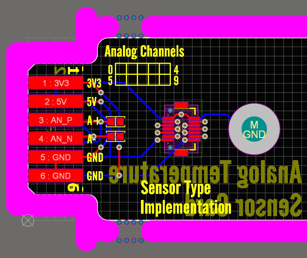
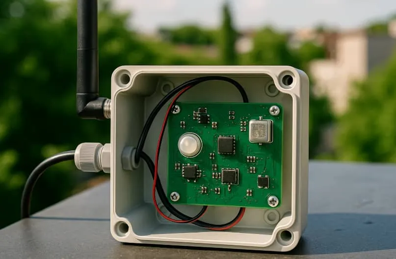
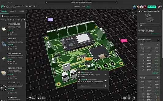
Microvia Design for EMI Reduction
Learn how microvia design can reduce EMI in PCB layouts. This guide covers technical principles, practical solutions, and industry standards to improve signal integrity and minimize noise in high density designs.
Master CT scanner PCB design with this detailed guide. Learn key principles of signal integrity, thermal management, and EMC shielding for high-reliability medical PCBs. Get practical tips for design and compliance.
Learn how 5G PCB layer stackup design boosts signal integrity and impedance control. Find practical tips on thicker copper layers and best practices to achieve reliable high frequency performance in 5G applications.
Optimize edge computing PCB design for medical diagnostics. Address tight power budgets, real-time data, RF integration, thermal control, and hardware security.
Learn practical 5G PCB layout design guidelines for engineers. This guide covers signal integrity, component placement, and industry standards to optimize high frequency performance and reliability in 5G applications.
Learn effective grounding strategies for EV battery management PCB design. Discover practical tips on ground plane setup, single-point grounding, and avoiding ground loops to ensure safety and performance in high-voltage systems.
Master 2oz copper PCB design with this detailed tutorial for beginners. Learn key principles, practical tips, and industry standards to create reliable high current boards for hobbyist projects with ease.
Learn the key differences between 1oz and 2oz copper PCBs to pick the best option for your project. Compare current capacity, thermal performance, and cost to ensure reliability and efficiency in your PCB design.
Learn how stacked microvias enhance HDI PCB design with compact layouts and improved signal integrity. Dive into technical benefits, challenges, and best practices for advanced electronics in this detailed guide for engineers.
Compare stacked via and via in pad technologies for BGA routing in PCB design. Learn their benefits, challenges, and best use cases for HDI PCB layouts to optimize component placement and signal integrity.
Learn proven methods for plating stacked vias to achieve uniform copper deposition. This guide covers key practices to avoid plating defects and ensure top quality in PCB manufacturing for reliable, high performance boards.
Learn how solder mask impacts thick copper PCBs with issues like adhesion and cracking. Find practical solutions to boost reliability in high power applications. Get expert tips for better PCB performance now.