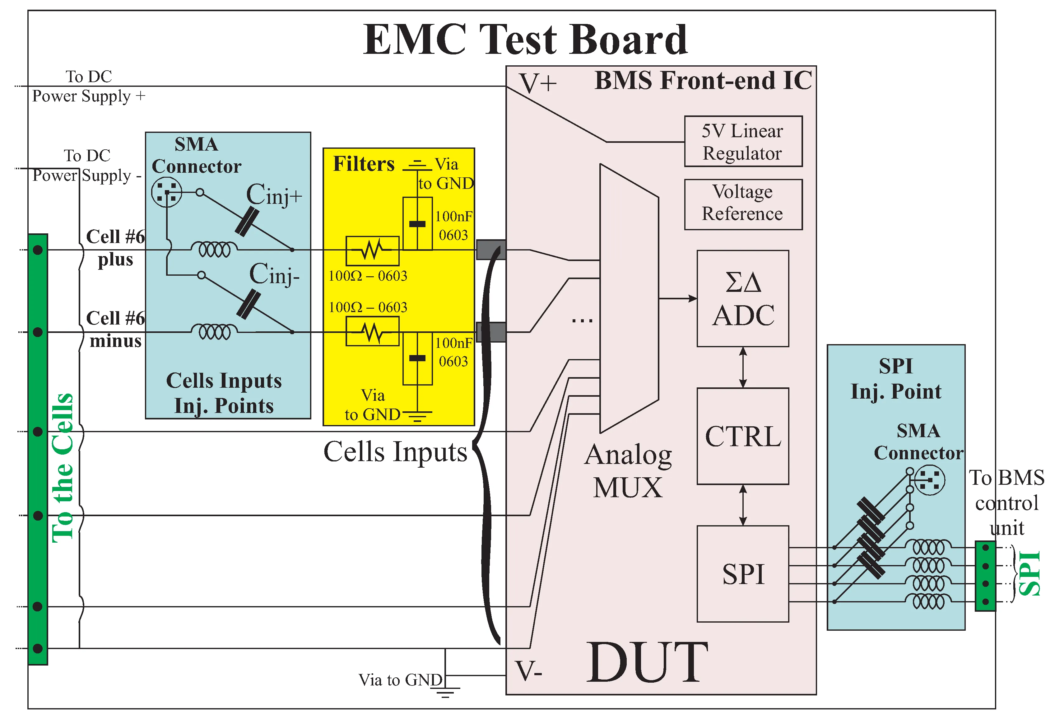
Help
  • FAQ
    browse most common questions
  • Live Chat
    talk with our online service
  • Email
    contact your dedicated sales:
0

PCB Knowledge

Printed circuit boards (PCBs) form the backbone of modern electronics, enabling everything from smartphones to industrial machinery. In our PCB Knowledge category, we delve into the essential principles, techniques, and innovations that drive this field forward. Whether you are an engineer refining your designs or a hobbyist embarking on your first project, this collection offers valuable resources to enhance your understanding and skills. The scope of PCB Knowledge spans foundational concepts such as circuit layout and component selection, extending to advanced topics like high-speed signal integrity and thermal management. We provide detailed guides that walk through design software usage, manufacturing processes, and quality assurance methods. Tutorials offer hands-on instructions for prototyping and assembly, while insights from industry experts share real-world case studies and emerging trends. Best practices emphasize reliability, cost efficiency, and compliance with standards like IPC, ensuring your projects meet professional benchmarks. The practical value lies in its direct applicability to everyday challenges. For instance, articles on troubleshooting common PCB failures can save time and resources in product development cycles. Discussions on materials science reveal how choices in substrates and coatings impact performance in harsh environments, such as automotive or aerospace applications. By addressing these elements, PCB Knowledge equips you with tools to innovate and optimize electronic systems that power renewable energy solutions, medical devices, and consumer gadgets. As you read through the articles here, you will gain a comprehensive perspective that connects theoretical knowledge with tangible outcomes. This category serves as a hub for ongoing learning, where each piece builds on the others to foster expertise in PCB technology. Stay informed on the latest advancements, from flexible PCBs to sustainable manufacturing, and apply these insights to your work for superior results.

 
High Density Interconnect (HDI) PCBs in MRI Machines: Advantages and Challenges
Signal Integrity HDI PCB PCB Design Tips

High Density Interconnect (HDI) PCBs in MRI Machines: Advantages and Challenges

HDI PCB for MRI machines pack more components into smaller spaces for superior signal integrity and reduced EMI in high-field scanners. Key advantages include density gains and reliability improvements. Challenges cover manufacturing costs microvias reliability and thermal issues. Review HDI PCB design rules and production best practices for electric engineers.

The Role of Multi Layer PCBs in Battery Charger Design: Advantages and Considerations
Signal Integrity Multilayer PCB Power Distribution EMI Reduction

The Role of Multi Layer PCBs in Battery Charger Design: Advantages and Considerations

Multi-layer PCB design offers key benefits for battery chargers, including signal integrity multi-layer control, power distribution multi-layer efficiency, and EMI reduction multi-layer shielding. This article details PCB stack-up strategies, design considerations, best practices, and FAQs for electric engineers building reliable systems. (198 characters)


2026 AIVON.COM All Rights Reserved
Intellectual Property Rights | Terms of Service | Privacy Policy | Refund Policy