Introduction
The rollout of 5G networks has transformed wireless communication, demanding printed circuit boards that handle frequencies from sub-6 GHz up to millimeter-wave bands beyond 24 GHz. High-frequency PCB design becomes critical to maintain signal integrity amid increased data rates and bandwidth requirements. Engineers face challenges like dielectric losses, impedance mismatches, and thermal buildup, which can degrade performance if not addressed early. This article explores key aspects of designing 5G PCBs, focusing on materials, stack-up strategies, impedance control, and thermal management. By following structured engineering principles, designers can ensure reliable operation in base stations, antennas, and user devices. Proper design not only meets performance goals but also aligns with manufacturing feasibility.
Why High-Frequency PCB Design Matters for 5G Applications
5G systems operate at much higher frequencies than previous generations, leading to shorter wavelengths and greater susceptibility to signal degradation. In high-frequency PCB design, even minor variations in material properties or trace geometry can cause reflections, crosstalk, or attenuation, compromising data throughput. For instance, millimeter-wave signals in 5G require precise control to avoid phase shifts that disrupt beamforming. This relevance extends to base stations and handsets, where PCB performance directly impacts network efficiency and coverage. Engineers must prioritize signal integrity from the schematic stage through fabrication. Ignoring these factors risks costly redesigns and field failures.
The shift to 5G also amplifies power densities, as more transceivers and amplifiers operate simultaneously. Thermal management for 5G PCBs emerges as a core concern, since heat affects material stability and signal propagation. Industry standards like IPC-2221 provide foundational guidelines for layer spacing and trace routing to mitigate these issues. Overall, robust high-frequency PCB design ensures 5G devices achieve low latency and high reliability in real-world deployments.
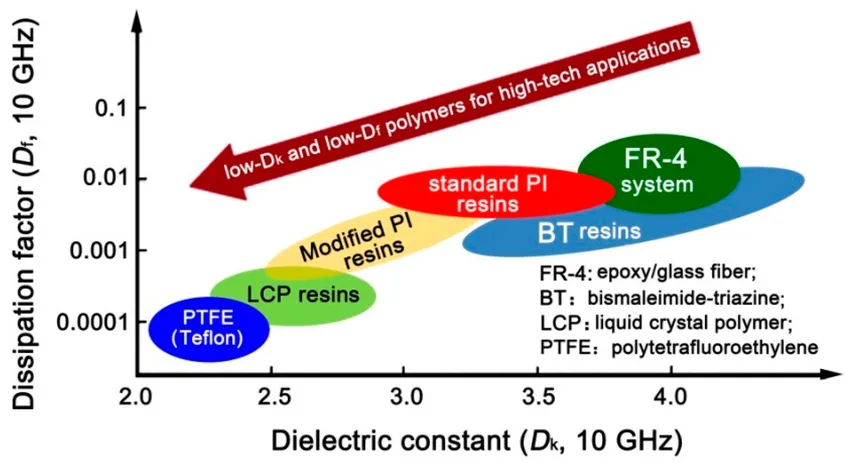
Selecting Low-Loss PCB Materials for 5G
Low-loss PCB materials for 5G feature low dielectric constant (Dk) and dissipation factor (Df) to minimize signal attenuation at high frequencies. Materials with stable Dk across temperature and frequency ranges prevent impedance drift, essential for consistent performance. Engineers select laminates that balance electrical properties with mechanical strength, avoiding those prone to moisture absorption which exacerbates losses. In practice, smoother copper surfaces reduce conductor losses, complementing the dielectric's low Df. Fabrication processes must preserve these properties during lamination and drilling. Engineers should evaluate proven high-frequency laminates in detail—see our dedicated guide on 5G Network PCB Materials: Selecting the Right Laminates for High-Frequency Performance.
Beyond basic specs, material compatibility with multilayer builds influences 5G PCB stack-up choices. Hybrid stacks combining low-loss cores with standard prepregs offer cost-effective solutions while maintaining signal integrity. Testing per IPC-6012 ensures qualification for high-frequency use, verifying dimensional stability under thermal stress. Designers iterate simulations to predict insertion loss before committing to prototypes. This approach optimizes both performance and manufacturability.
Here is a comparison of common materials used in 5G PCB design:
Material Comparison Table
| Material | Dk @10 GHz | Df @10 GHz | Moisture Absorption (%) | Approx. Loss @28 GHz (dB/in) | Relative Cost | Best Applications |
|---|---|---|---|---|---|---|
| Standard FR-4 | 4.3–4.5 | 0.018–0.022 | ~0.10 | >1.5 | Low | Digital only – avoid for mmWave |
| Rogers RO4350B | 3.48 | 0.0037 | 0.06 | ~0.55 | Medium | Sub-6 GHz AAU, MIMO antennas, general RF |
| Panasonic Megtron 6 | 3.4–3.6 | 0.002 | 0.05 | ~0.45 | Medium-High | High-speed mixed-signal, baseband + RF |
| Isola Astra MT77 | 3.00 | 0.0017 | <0.10 | ~0.40 | High | mmWave small cells, 28–39 GHz designs |
| Rogers RT/duroid 5880 | 2.20 | 0.0009 | 0.02 | ~0.30 | Very High | Pure mmWave antennas, lowest-loss phased arrays |
Impedance Control in 5G PCBs: Principles and Techniques
Impedance control in 5G PCBs requires precise calculation of characteristic impedance based on trace width, thickness, spacing, and surrounding dielectrics. At high frequencies, mismatches cause reflections that distort eye diagrams and increase bit error rates. Engineers use field solvers to model single-ended and differential pairs, accounting for frequency-dependent effects like skin effect. Maintaining 50-ohm or 100-ohm targets demands tight tolerances, often within 10% variation. Routing strategies minimize vias and bends, which introduce discontinuities.
Reference planes adjacent to signal layers provide return paths, reducing radiation and crosstalk. In impedance control in 5G PCBs, coplanar waveguides or striplines suit different sections, chosen per signal speed. Prepreg selection fills gaps uniformly to avoid air pockets that alter effective Dk. Fabrication feedback loops refine models, ensuring production boards match simulations. IPC-2221 outlines design parameters for controlled impedance, emphasizing symmetry in stack-up.
Optimizing 5G PCB Stack-up for Performance
A well-planned 5G PCB stack-up balances signal integrity, power delivery, and thermal dissipation across multiple layers. Symmetric constructions prevent warpage, with core and prepreg thicknesses mirroring from the center. High-speed signals pair with ground planes to form striplines, isolating them from crosstalk sources. Power planes interleave strategically, providing low-inductance paths while respecting clearance rules. Typical 5G builds use 10 or more layers to segregate RF, digital, and DC sections. A well-balanced multilayer configuration is essential; refer to our analysis of layer stackup design for optimum 5G performance for practical examples.
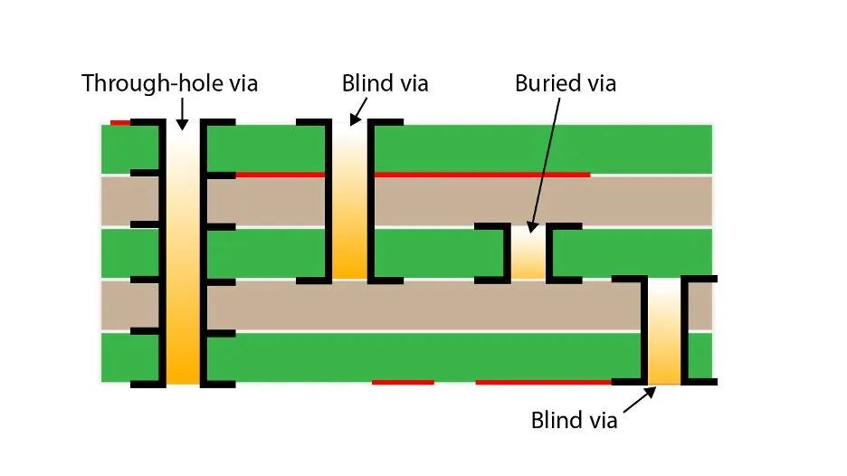
In 5G PCB stack-up design, via transitions demand blind or buried types to shorten stub lengths, preserving high-frequency response. Aspect ratios stay below 10:1 for reliable plating. Simulations predict resonance modes, guiding layer assignments. Mechanical stability improves with balanced copper distribution, aligning with IPC-6012 performance specs. Engineers document stack-up details for fabricators, including material callouts and press cycles.
Example 8-Layer Hybrid Stack-Up for 5G mmWave + Digital Board
| Layer | Type | Material | Thickness (approx.) | Purpose |
|---|---|---|---|---|
| 1 | Signal | Rogers RO4350B | 0.008" | mmWave/RF traces, antenna feeds |
| 2 | GND | Copper | 1 oz | Solid reference for Layer 1 |
| 3 | Signal | Rogers or Megtron | 0.006" | Stripline high-speed signals |
| 4 | GND/Power | Copper | 1 oz | Reference + power delivery |
| 5 | Power/GND | Copper | 1 oz | Symmetric power plane |
| 6 | GND | Copper | 1 oz | Reference for Layer 7 |
| 7 | Signal | Standard | 0.008" | Digital/control routing |
| 8 | Signal/GND | Standard | 0.008" | Bottom components or ground |
Via Optimization, Back-Drilling & Discontinuity Mitigation
Vias are major sources of discontinuity in mmWave designs. A through-hole via stub acts as an open transmission line stub that creates resonant notches, severely degrading return loss above 20 GHz.
Recommended strategies for 5G PCBs:
- Use blind, buried, or microvias to eliminate stubs.
- Back-drill through-hole vias to remove unused portions (target stub <10% of wavelength).
- Space ground stitching vias at ≤ λ/20 at the highest frequency of interest for effective shielding.
- Optimize via aspect ratios (<10:1) and pad sizes to reduce capacitance.
- Back-drill or use skip vias for critical transitions.
- Model via transitions in 3D EM simulators to compensate with anti-pads or ground cutouts.
Thermal Management for 5G PCBs
Thermal management for 5G PCBs addresses heat from power amplifiers and dense ICs operating at elevated frequencies. High power densities demand vias arrays under hotspots to conduct heat to inner planes or outer spreads. Material choices with higher glass transition temperatures resist delamination under cycling. Copper thickness increases in power layers enhance spreading without excessive weight. Simulations using finite element analysis predict hotspots, informing via fencing and cutouts.
Convection and conduction paths integrate via board stiffeners or embedded heatsinks. In thermal management for 5G PCBs, phase change or gap fillers bridge components to chassis, but PCB-level design sets the foundation. Standards guide via reliability under thermal shock. Monitoring junction temperatures ensures operation within component ratings. This holistic approach sustains performance over device lifecycle.
Best Practices for Signal Integrity in High-Frequency Design
Routing high-frequency traces follows length-matching for differential pairs to preserve timing skew. Minimize discontinuities with back-drilling or laser vias, critical for multi-gigabit links. Ground stitching vias along edges shield against EMI. Decoupling capacitors place near pins reduce noise coupling into signals. Post-layout extraction verifies S-parameters against margins.
Length tuning serpentine patterns avoid sharp bends that radiate. Fabricators control etch uniformity for consistent widths. Signal integrity analysis tools flag violations early. These practices ensure 5G PCBs meet eye height and jitter specs.
Challenges of High-Frequency Signals in 5G Applications
At mmWave frequencies, wavelengths shrink dramatically (approximately 10–12 mm at 28 GHz), making even minor variations in trace geometry, material properties, or manufacturing tolerances highly impactful. Signals experience greater attenuation, with standard FR-4 materials exhibiting losses exceeding 1.5–2 dB per inch at 28 GHz. In contrast, optimized low-loss materials can reduce this to under 0.5 dB per inch.
Key challenges in 5G PCB design include:
- Attenuation and dielectric loss: Energy dissipates as heat in the substrate and conductor.
- Reflections and impedance discontinuities: These distort eye diagrams and raise bit error rates.
- Crosstalk and EMI: Tighter routing density and higher power amplify coupling.
- Increased power density: Multiple transceivers and power amplifiers operating simultaneously create thermal hotspots that further degrade material stability and signal propagation.
These issues appear in base stations, small cells, and handsets, directly affecting latency, coverage, and reliability. Early attention to signal integrity—from schematic through fabrication—prevents costly redesigns. Industry standards such as IPC-2221 and IPC-6012 provide baseline guidance, but real-world 5G performance demands simulation-driven, application-specific optimization.
Conclusion
Designing 5G PCBs for high-frequency performance demands integrated attention to low-loss materials, precise impedance control, optimized stack-ups, and robust thermal management. Engineers achieve signal integrity through simulation-driven choices and standards adherence. Practical implementation minimizes losses, reflections, and heat, enabling reliable 5G deployment. Future iterations will refine these principles as frequencies rise. Prioritizing these elements from concept to production yields superior outcomes. For foundational concepts, start with our high frequency PCB design for beginners.
FAQs
Q1: What are the key characteristics of low-loss PCB materials for 5G?
A1: Low-loss PCB materials for 5G exhibit low dissipation factor and stable dielectric constant across wide frequencies and temperatures. They minimize insertion loss in millimeter-wave bands, supporting high data rates. Smoother copper foils complement the dielectric to reduce skin effect losses. Selection balances cost with performance in multilayer builds. Proper handling preserves properties during processing.
Q2: How do you achieve impedance control in 5G PCBs?
A2: Impedance control in 5G PCBs involves modeling trace geometry, dielectrics, and planes using field solvers. Target tolerances like +/-10% through uniform etching and stack-up symmetry. Adjacent ground planes stabilize return paths for high frequencies. Minimize vias and use differential routing for balanced lines. Verify with TDR measurements post-fabrication.
Q3: Why is 5G PCB stack-up critical for signal integrity?
A3: 5G PCB stack-up isolates high-speed signals with dedicated plane pairs, reducing crosstalk and EMI. Symmetric layering prevents warpage and maintains impedance. It accommodates dense routing while providing power integrity. Via optimization shortens transitions for minimal reflections. Balanced copper distribution aids thermal flow.
Q4: What strategies improve thermal management for 5G PCBs?
A4: Thermal management for 5G PCBs uses thermal vias, thicker copper planes, and material stability to dissipate heat from amplifiers. Simulate hotspots to place relief strategically. Integrate conduction paths to chassis. Avoid hotspots near sensitive RF traces. Cycle testing validates long-term reliability.
References
IPC-2221B — Generic Standard on Printed Board Design. IPC, 2003
IPC-6012E — Qualification and Performance Specification for Rigid Printed Boards. IPC, 2015
IPC-A-600K — Acceptability of Printed Boards. IPC, 2020