Hard gold plating thickness is a key specification for FPC gold fingers used in repeated-mating connectors. The correct thickness depends on the expected mating cycles, connector contact conditions, nickel underplate, and the manufacturing process used to control the plated surface. A thicker gold layer is not automatically better; the specification needs to balance wear resistance, flexibility, dimensional requirements, and production capability.
In production, AIVON evaluates FPC hard gold thickness against the customer's connector requirements and expected insertion life. CAM engineers review the drawing, plating specification, and mating-cycle requirement before setting the process target. When the requirement is unclear, the thickness is flagged for engineering confirmation rather than being treated as a generic value.
How Hard Gold Plating Thickness Affects FPC Gold Finger Life
For FPC gold fingers used in repeated-mating connectors, hard gold plating thickness directly affects how long the contact surface can withstand mechanical wear. Every insertion and removal cycle creates wiping friction between the gold finger and the connector contact. If the plated layer is too thin for the required service life, the underlying nickel layer can eventually become exposed and contact performance may become less stable.
However, choosing the thickest possible gold layer is not the correct approach. The required thickness should be based on the expected mating cycles, connector contact force, operating environment, and the construction of the flexible circuit.
Match Gold Thickness to the Required Mating Cycles
The first question during complex flexible pcb design should be how often the connector will be mated and unmated.
A flexible circuit used as a permanent connection may have very different requirements from an FPC that is regularly removed for service, testing, battery replacement, or module replacement. High-cycle interfaces need a plating specification that can withstand repeated mechanical wiping without premature wear.
For this reason, gold finger plating thickness should be specified together with the expected mating life rather than treated as an isolated material parameter.
The connector manufacturer's requirements should also be reviewed. Contact force, contact geometry, insertion depth, and the direction of wiping can all influence how quickly the plated surface wears.
Consider the Entire Contact Structure
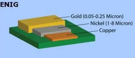
Gold is only the top layer of the contact structure. Beneath it, the nickel underplate provides a barrier and mechanical foundation.
The finished structure can therefore be considered as:
Copper → Nickel → Hard Gold → Connector Contact
If the gold layer wears through, the nickel layer becomes part of the electrical contact interface. This can change contact behavior and accelerate degradation depending on the connector construction and environment.
For demanding applications, the engineering review should therefore consider FPC hard gold thickness, nickel thickness, finished finger thickness, and connector requirements together.
Why Thicker Gold Is Not Always Better
A thicker gold layer can increase wear resistance, but it also increases plating cost and may affect dimensional control. On a flexible PCB circuit, excessive plating can also become a concern when the finger area is integrated with stiffeners, coverlay openings, or tightly controlled insertion dimensions.
The objective is not to maximize gold thickness. It is to establish a plating window that provides sufficient wear resistance while remaining compatible with the mechanical and dimensional requirements of the FPC.
For applications requiring a high reliability gold bonding FPC, the gold specification should likewise be evaluated together with mechanical loading, environmental conditions, interface design, and required service life rather than selected from thickness alone.
How FPC Hard Gold Thickness Is Controlled During Plating
The value specified on an FPC drawing is a finished-product requirement, but the manufacturer must control several process variables to achieve that result consistently.
During production, FPC hard gold thickness can vary across the panel because current distribution, plating area, trace geometry, and local feature density are not identical everywhere. A process target therefore needs to account for normal manufacturing variation.
Set the Plating Target Above the Minimum Requirement
If the drawing specifies a minimum finished gold thickness, the production target cannot simply equal that minimum.
A manufacturing process normally needs an internal target above the lower specification limit so that normal variation does not cause finished parts to fall below the customer's requirement.
For example, if the drawing defines a minimum gold thickness, the plating team may establish a controlled process target that provides enough margin for panel-to-panel and position-to-position variation.
The exact target depends on the plating process, panel design, specification, and manufacturer's process capability.
Control Current Density and Plating Distribution
Electrolytic hard gold plating depends on current distribution across the panel. Areas with different geometries or distances from the electrical connection can experience different deposition behavior.
Finger width, spacing, copper distribution, plating bus design, and panel arrangement can therefore influence the final FPC gold plating thickness.
This is one reason why the plating requirement should be reviewed during CAM preparation rather than treated as a simple purchasing specification.
A good CAM review can identify areas where the panel design may create unusually high or low plating deposition and allow the manufacturer to compensate before production.
Consider the Nickel Underplate
The nickel layer beneath the gold should be controlled as part of the complete plating structure.
Nickel provides a barrier between copper and gold and contributes to the mechanical stability of the contact finish. The required nickel thickness depends on the application and manufacturing specification.
For FPC gold fingers, the nickel and gold specifications should therefore be defined together. Optimizing only the gold layer while ignoring the underlying nickel structure can produce an incomplete plating specification.
What Happens When FPC Gold Plating Thickness Is Too Thin or Too Thick
The effects of incorrect FPC gold plating thickness are not limited to material cost. An unsuitable specification can influence contact reliability, wear resistance, dimensional control, and production consistency.
Problems Caused by Insufficient Gold Thickness
If the gold layer is below the required thickness for the application, repeated connector insertion can accelerate surface wear.
Potential consequences include:
- premature exposure of the nickel underlayer
- increased contact resistance
- intermittent electrical contact
- reduced mating-cycle life
- greater sensitivity to mechanical wear
The actual failure mechanism depends on the connector and operating environment, so these effects should not be assumed for every FPC design.
The key point is that the specified hard gold plating thickness needs to match the mechanical demands of the contact interface.
Problems Caused by Excessive Gold Thickness
Increasing gold thickness beyond the application's requirement can also create problems.
The most obvious impact is higher material and processing cost. Excessive plating may also complicate finished-thickness control when the FPC finger area must fit into a connector with a tight dimensional window.
For an FPC, the gold finger is only one part of the finished flex PCB assembly. The total insertion thickness may also include the copper, dielectric layers, coverlay, adhesive, stiffener, and plated finish.
Therefore, the gold specification should be considered together with the complete insertion interface.
Check the Connector Before Increasing Plating Thickness
When a customer requests a higher gold thickness because of reliability concerns, the manufacturer should first confirm what failure mechanism the increased thickness is intended to address.
For example, the actual issue may involve:
- excessive connector contact force
- incorrect insertion depth
- insufficient stiffener support
- poor finger geometry
- repeated misalignment
- environmental exposure
- inadequate nickel specification
In these situations, simply increasing gold thickness may not solve the underlying problem.
Where the process window forces thickness decisions during panel plating
Hard gold on FPC is electrolytic, selective, and run after the coverlay is already laminated. The polyimide and adhesive outgas slightly in the plating tanks, so bath chemistry drifts faster than on rigid boards. Current density across a flex panel is also less uniform because the material is thin and can float or wrinkle on the plating rack. That combination means the gold thickness variation across a single panel is typically ±15–20 %. If the designer asks for 0.3 µm minimum, the process must target 0.4–0.45 µm average just to keep the low points above 0.3 µm. That is why CAM engineers rarely accept a 0.3 µm call-out without an explicit "minimum after plating" note; otherwise the plating line will push the average higher to protect yield.
Nickel thickness is less variable but still critical. Below 3 µm the nickel becomes discontinuous on the rolled-annealed copper used for most FPCs; above 6–7 µm the flex becomes stiffer and the gold finger can crack when the cable is bent near the connector. Production therefore holds nickel between 3 µm and 5 µm and only opens the window for high-reliability or thick-gold builds.
How Manufacturers Control Hard Gold Plating Thickness on FPCs
Achieving consistent hard gold plating thickness requires control from engineering review through final inspection. A reliable process does not depend on a single thickness measurement at the end of production.
Review the Gold Finger Area During CAM
Before production, the CAM team should confirm:
- gold finger dimensions
- finger spacing
- plating area
- coverlay opening
- stiffener construction
- finished insertion thickness
- nickel and gold requirements
- connector-related tolerances
The goal is to make sure the drawing specification can be translated into a stable manufacturing process.
If the required plating thickness is unclear or conflicts with the finished dimensional requirement, the issue should be resolved during engineering review rather than after fabrication.
Control Plating Conditions During Production
During plating, the production team needs to maintain consistent process conditions.
Relevant factors can include:
- current density
- plating time
- bath condition
- temperature
- chemical concentration
- panel loading
- electrical contact
- panel geometry
These variables influence deposition rate and distribution. A stable process helps keep FPC hard gold thickness within the required specification across production batches.
Verify Thickness With XRF Measurement
X-ray fluorescence (XRF) is commonly used to measure plated-metal thickness without destroying the finished FPC.
For gold fingers, measurements can be taken at representative locations to verify that the plating process is producing the required thickness.
Measurement points should be selected carefully because plating distribution may vary across a panel. When the application has tight reliability requirements, the inspection plan should define the measurement locations and acceptance criteria before production begins.
Compare the Finished Result With the Drawing
Final inspection should not only confirm that gold is present. The measured gold finger plating thickness should be compared with the drawing requirement and the manufacturer's internal process target.
This provides a more useful production-control loop:
Customer specification → CAM review → plating target → production control → XRF measurement → final verification
This approach helps identify process drift before it becomes a recurring quality problem.
Conclusion
Choosing the right hard gold plating thickness for FPC gold fingers is not simply a matter of making the gold layer thicker. The specification should match the expected mating cycles, connector design, nickel underplate, finished insertion thickness, and operating environment. A well-controlled plating process, combined with CAM review and XRF inspection, helps maintain consistent contact performance and avoid unnecessary plating cost.
For demanding FPCB applications, AIVON reviews the gold finger structure and plating requirements during engineering and manufacturing to ensure the finished FPC meets the intended mechanical, electrical, and reliability requirements.
FAQ
Q1: Can FPC gold fingers be plated selectively?
A1: Yes. Hard gold can be applied selectively to the FPC areas that require repeated electrical contact, while other exposed areas can use a different surface finish when appropriate. Selective plating can help control manufacturing cost and keep the plating specification focused on functional contact areas.
Q2: Does an FPC need a stiffener under the gold fingers?
A2: A stiffener is commonly used when the FPC gold finger must meet a specific insertion or connector-interface requirement. It increases local mechanical support and helps maintain the dimensional stability of the insertion area. The stiffener material and thickness should be selected according to the connector design and the required finished thickness.
Q3: Can gold fingers be placed directly next to the FPC bending area?
A3: Gold fingers are normally located in a controlled insertion area rather than directly within a highly dynamic bending zone. The transition between the rigid contact area and flexible section should be considered during layout so that bending stress is not concentrated at the connector interface.
Q4: How does coverlay affect FPC gold finger design?
A4: Coverlay must be opened around the contact area so that the gold fingers can engage properly with the connector. The coverlay opening, finger length, edge clearance, and registration tolerance should be reviewed together because insufficient clearance can interfere with insertion or reduce the effective contact area.
Q5: What FPC dimensions are important for connector insertion?
A5: Important dimensions can include overall FPC thickness, gold finger length and width, finger spacing, edge geometry, stiffener thickness, and the position of the coverlay opening. These dimensions should be matched to the connector manufacturer's recommended insertion envelope rather than defined independently.
Q6: Can FPC gold fingers be used with both ZIF and non-ZIF connectors?
A6: Yes, but the mechanical requirements are different. ZIF connectors typically use a locking mechanism to secure the FPC, while other connector designs may rely more heavily on contact force and insertion geometry. The FPC finger dimensions and supporting structure should therefore be designed for the specific connector interface.
Q7: What materials are commonly used for FPC gold finger stiffeners?
A7: Common stiffener options include FR-4, polyimide, and stainless steel. The appropriate material depends on the required insertion support, thickness tolerance, flexibility, temperature conditions, and available space around the connector. Material selection should be considered together with the overall FPC construction.
Q8: What information should be provided when ordering an FPC with gold fingers?
A8: The manufacturing package should clearly identify the gold finger location, contact dimensions, surface-finish requirement, finished FPC thickness, stiffener specification, coverlay opening, connector information, and any special dimensional tolerances. Providing the connector part number or manufacturer's drawing can also help the PCB manufacturer verify the interface before production.
Q9: Can the same gold finger design be used for different FPC connectors?
A9: Not necessarily. Even when two connectors appear similar, their insertion depth, contact geometry, locking method, pitch, and dimensional tolerances may differ. The gold finger layout should therefore be checked against the specific connector rather than reused solely based on pitch or appearance.
Q10: What should be checked before manufacturing an FPC with gold fingers?
A10: Before fabrication, the manufacturer should review the connector drawing, gold finger geometry, coverlay opening, stiffener dimensions, finished thickness, bend-area transition, and plating specification. A pre-production DFM review can identify interface conflicts before the FPC enters fabrication.