In flexible PCB coverlay design, the opening size is not a free variable. When the coverlay window is drawn significantly larger than the copper pad it is meant to expose, the immediate result is unprotected copper around the pad perimeter. That annular ring of bare or poorly protected copper is where most of the downstream problems start.
Coverlay is laminated polyimide film with adhesive. Unlike liquid photoimageable solder mask, it is cut first (laser or mechanical) and then aligned and pressed. Registration is never perfect. Adhesive still flows. Designers who open the coverlay far beyond the necessary clearance to "be safe" usually create more risk than they eliminate.
Why Oversized Coverlay Openings Leave Pads and Traces Exposed
Typical production capability sits around ±0.05 mm for laser-cut coverlay and ±0.10–0.15 mm for punched. Adhesive squeeze-out adds another 0.05–0.10 mm of effective encroachment under normal lamination pressure. The industry response is a designed oversize of roughly 0.075–0.125 mm per side (0.15–0.25 mm total). That window absorbs the process variation and still leaves the full pad solderable.
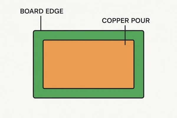
When the opening is drawn much larger—0.3 mm or more per side—the excess copper stays permanently outside the coverlay edge. Surface finish may cover the pad itself, but the annular ring often receives incomplete or zero finish protection depending on how the plating process is masked. The copper is simply sitting there.
That is the core design mistake: treating coverlay opening size as a generous access hole instead of a controlled clearance feature.
Copper Oxidation and Environmental Degradation Risks
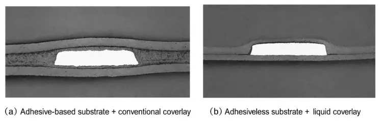
Exposed copper oxidizes. On a rigid board with solder mask the risk is usually limited. On an FPC the situation is worse. The circuit flexes, the coverlay edge lifts microscopically under repeated strain, and moisture or ionic contaminants reach the copper more readily.
In practice the oxidation starts at the coverlay-to-copper transition. Once the oxide layer forms, it can propagate under the coverlay edge, reducing adhesion. In high-humidity or outdoor applications the exposed ring becomes a preferential corrosion site. Even with ENIG or immersion silver on the pad, the unprotected copper just outside the designed land often shows discoloration within weeks of storage if the opening was excessive.
Long-term reliability takes the hit first. Intermittent contact resistance or open circuits after thermal cycling are common observations when the coverlay opening leaves too much copper free.
Pad Mechanical Support and Flex Fatigue
Coverlay does more than insulate. It anchors the copper. When the opening is oversized, the pad edge loses that mechanical clamp. Under dynamic flex the stress concentrates exactly at the coverlay termination line. Copper fatigue cracks initiate there far earlier than on a properly sized opening.
The same mechanism appears around unsupported pads or gold-finger roots. Designers who enlarge the opening to guarantee full exposure often remove the very overlap that prevents pad lift or trace fracture during handling and assembly.
Large continuous openings also distort during lamination. Polyimide film stretches. An opening longer than roughly 20–25 mm frequently wrinkles or shifts, creating local adhesion voids that further expose copper.
Assembly and Solder Process Consequences
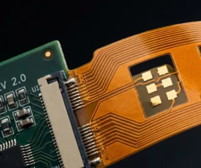
Stencil design assumes a known land geometry. An oversized coverlay opening changes the effective solderable area and the surface energy at the pad perimeter. Excess paste volume, uncontrolled wicking along the exposed copper, or solder bridging to nearby features become more likely when the coverlay edge is far from the pad.
In fine-pitch areas the problem compounds. The minimum clearance from coverlay opening edge to adjacent copper is typically held at 0.15 mm. An oversized opening easily violates that spacing once registration tolerance is applied, leaving a path for solder shorts.
AOI and visual inspection also suffer. The large copper ring looks like a defect to operators trained on standard pad-to-coverlay relationships, generating false rejects or, worse, missed real defects.
Practical Rules for Controlling FPC Coverlay Opening Size
Start with the pad, not with a generic expansion rule copied from rigid boards.
Design the coverlay opening 0.075–0.125 mm larger than the copper pad on each side for standard laser processes. Confirm the exact capability with the fabricator; some laser lines hold tighter, some punched processes need more. Never default to 0.3 mm or larger "just to be safe."
Maintain ≥0.15 mm clearance from the finished opening edge to any adjacent copper feature. That number already includes typical registration variation.
Radius every internal corner of the opening—minimum 0.2 mm. Sharp corners act as stress risers and also tear more easily during film handling.
Limit continuous opening length. Above 20–25 mm, split the window or add coverlay bridges if the design allows. Large open areas wrinkle under heat and pressure.
For fine-pitch or high-reliability work, specify laser cutting in the fabrication notes and request the actual measured registration capability. Do not assume the nominal oversize will survive the process without verification.
Engineering Takeaway on Coverlay Opening Control
FPC coverlay opening size is a balance between ensuring full pad exposure and limiting unprotected copper. Too small and adhesive or misalignment steals solderable area. Too large and the copper sits open to oxidation, mechanical fatigue, and process variability.
The correct window is narrow and process-specific. Design it from the copper pad outward using the fabricator's real registration and adhesive-flow numbers, keep adjacent clearances intact, and avoid treating the coverlay opening as an oversized access hole. That single discipline removes most of the oxidation, reliability, and assembly issues that appear when the opening is simply drawn too large.