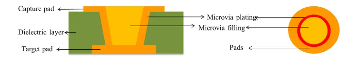
In production we treat microvia landing pad failure as a registration-and-capture problem first. CAM engineers open the design, measure the target pad diameter against the laser drill size plus the actual layer-to-layer registration budget, and either enlarge the pad or reject the file. If the pad is already fixed, we shift the laser program or adjust the panel compensation so the via still lands fully on copper. Plating parameters are locked to guarantee sidewall and bottom coverage once the via is drilled. That is the working rule on the floor.
How pad size and registration stack up against laser accuracy
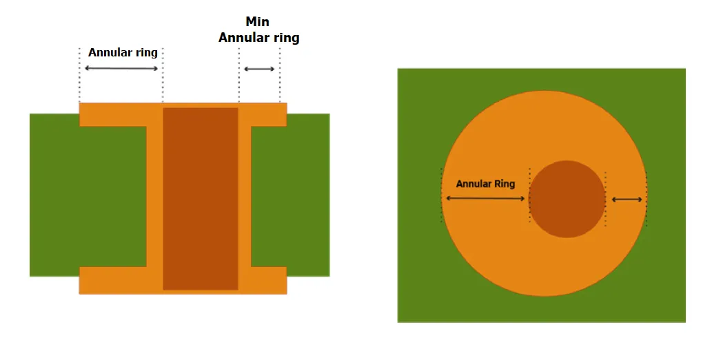
Microvia landing pad failure shows up most often when the capture pad is sized too close to the finished via diameter. A typical 75 µm or 100 µm laser via needs a target pad that already accounts for the cumulative registration tolerance of the outer-layer image, the inner-layer image, and the laser drill itself. On most HDI lines that stack is ±25 µm to ±40 µm under good conditions and can reach ±50 µm or more when the panel is large or the material is high-Tg. If the designer leaves only 25 µm annular ring on each side, the via edge walks off the pad copper on a measurable percentage of the panel.
Copper thickness on the landing layer adds another variable. When the foil is thin (9 µm or 12 µm) the laser can over-ablate and create a small crater at the pad surface. When the foil is thick (18 µm or more) residual copper can remain at the bottom of the via, reducing the contact area that plating has to cover. Either condition reduces the effective landing zone and turns a marginal registration offset into an open or high-resistance connection.
What the process does when the via walks off the pad
Once the laser hits dielectric instead of copper, the subsequent desmear and electroless copper steps have nothing solid to build on. Electroless coverage becomes patchy, electrolytic plating grows thinner or stops, and the finished via shows a partial or complete break at the pad interface. On the electrical test this appears as opens or intermittent contacts. On the assembly side the same defect can survive initial test and fail after thermal cycling or vibration because the remaining copper bridge is mechanically weak.
Yield impact is not uniform across the panel. The center of the panel usually stays within tighter registration, so the failures concentrate toward the edges and corners. That pattern makes the problem easy to miss on small test coupons and hard to contain once the full production lot is running. Scrap or rework then delays the shipment because the entire panel or the entire lot has to be held until the root cause is confirmed.
CAM and process controls that keep the via on copper
On the CAM side the first filter is a hard annular-ring check. Most factories set a minimum capture-pad diameter of via size + 50 µm to + 80 µm total (25–40 µm per side) for sequential build-up layers. When the incoming design is below that number we enlarge the pad if space allows, or we flag the job for customer confirmation. If enlargement is blocked by clearance rules we apply a global or local compensation shift to the laser drill program so the nominal via center moves toward the actual pad location measured on the imaged panel.
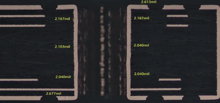
During laser processing we run a first-article registration check using either optical targets or a small set of test vias that are then cross-sectioned. If the measured offset exceeds the allowed budget we re-scale or re-offset the drill file before releasing the full panel. Copper thickness on the landing layer is controlled by the previous plating or foil specification; we do not accept a landing foil thinner than the process window that was qualified for that laser recipe.
Plating coverage is protected by two process locks. Desmear time and chemistry are tuned so the dielectric is cleaned without undercutting the copper pad edge. Electroless copper deposition is monitored for bottom-of-via coverage; if the coverage drops below the internal limit the panel is stripped and reworked rather than pushed forward. Electrolytic plating then builds the via fill or conformal copper under controlled current density so the interface remains continuous.
When the factory will accept a tighter landing pad
Exceptions are granted only when the design uses a smaller panel size, a tighter registration process (for example sequential build-up with optical alignment on every layer), and a laser system that has demonstrated ±20 µm or better capability on that material. In those cases the minimum annular ring can be reduced to 15–20 µm per side, provided the customer accepts the lower process window and the higher risk of edge-of-panel yield loss. Thick copper landing pads or designs that already include redundant microvias in parallel are also allowed more latitude because a single partial connection does not open the net.
Outside those conditions the pad size and registration rules stay firm. Microvia landing pad failure is almost always the result of the via edge leaving the copper; the practical solution is to keep enough copper under the laser and to confirm that coverage with plating controls before the panel leaves the HDI line.