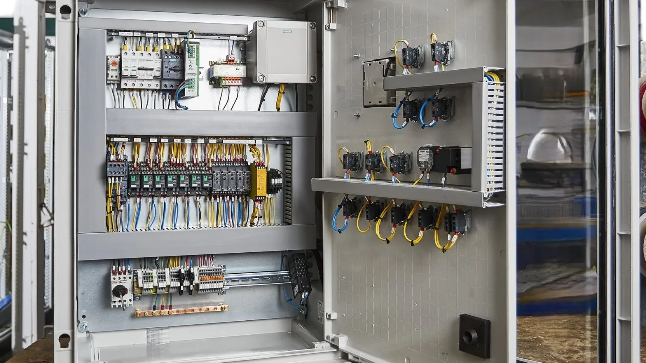
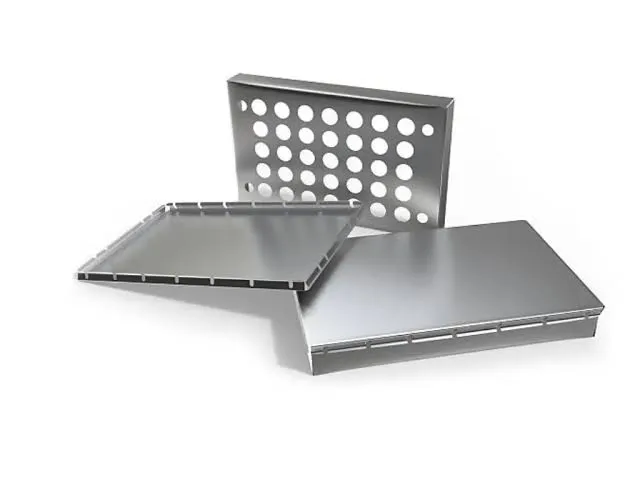
In production we treat sheet metal enclosure EMI shielding as a system-level contact problem rather than a standalone mechanical feature. When a PCB arrives with notes that it must sit inside a metal box for EMI performance, CAM first checks the peripheral copper, ground via density, and any edge features that will mate against the enclosure walls or conductive gaskets. We force continuous ground pour to the board edge wherever the mechanical drawing shows contact points, and we add via stitching at 3–5 mm pitch along those edges so the finished board can form a low-impedance path into the Faraday cage. If the enclosure drawings show multiple panels or lids, we also flag any copper voids under gasket landing zones because those voids become the first leakage path once the box is closed.
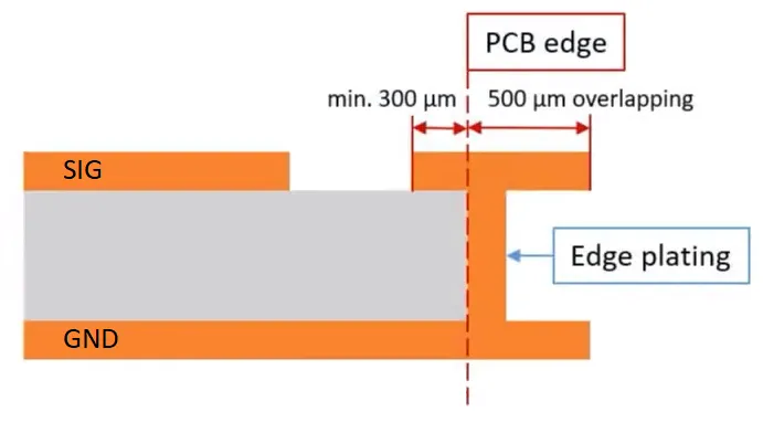
Where copper discontinuity at the board edge creates the first leakage path
The issue shows up because sheet-metal enclosures rely on the PCB itself to complete the shield at every interface. Fabrication tolerances on etch, plating thickness, and soldermask registration routinely leave 50–100 µm of copper pull-back or soldermask encroachment at the board outline. When that edge is supposed to press against a conductive gasket or directly against the metal wall, the resulting gap acts like a slot antenna. At the same time, panel routing and V-score processes introduce edge roughness that further reduces reliable contact area. Material expansion during reflow and subsequent temperature cycling opens those micro-gaps even more, so what looked continuous in the CAD file becomes intermittent once the board is inside the enclosure.
Ground plane splits or isolated copper islands near the perimeter compound the problem. Any break in the ground return path forces return current to travel longer loops, raising the impedance that the enclosure is trying to short out. In high-volume runs we see this most clearly on boards that pass free-space radiated tests yet fail once the same board is locked inside the metal box, because the enclosure now amplifies the residual common-mode current that the discontinuous copper allowed to escape.
What leakage through seams and openings does to yield and shipment
When the copper-to-enclosure interface is left uncontrolled, the first production symptom is a sudden drop in shielding effectiveness between 100 MHz and 1 GHz. Seams that rely on simple screw pressure without conductive gasket material open under vibration and thermal cycling; the residual slot radiates. Apertures larger than roughly λ/20 for the highest frequency of interest become efficient antennas, so any ventilation hole, display cut-out, or connector opening that is not treated with a waveguide-beyond-cutoff or conductive mesh pushes the board past regulatory limits. In practice this shows up as 6–15 dB worse radiated emissions once the unit is assembled, forcing either a re-spin of the PCB ground strategy or a mechanical rework of the enclosure that delays the entire shipment lot.
On the PCB side the same leakage drives higher return rates after the customer's system-level EMI scan. Boards that looked good in the fab's own near-field scan fail once the sheet-metal lid is closed because the lid now couples energy that previously radiated freely. Scrap and rework costs climb quickly when every unit must be opened, gasket replaced, or additional grounding screws added on the production line.
How CAM and process control close the shield in real builds
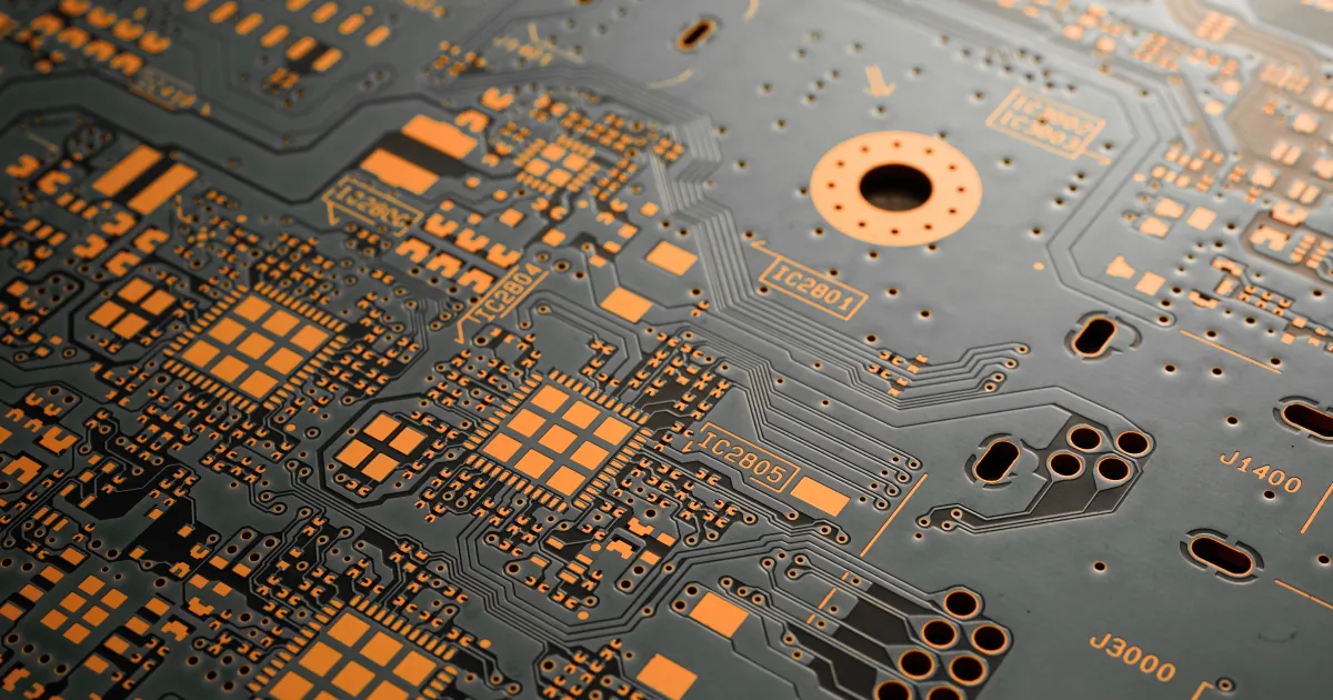
Most factories handle the copper side by enforcing a continuous ground pour to within 0.2 mm of the board outline on every layer that mates to the enclosure. Via stitching is added at 4 mm nominal pitch along the entire contact perimeter; the vias are tented on the outer layers so soldermask does not create an insulating film under the gasket. Where the mechanical design calls for conductive elastomer or finger-stock gaskets, we open soldermask windows over the copper so the gasket lands directly on bare metal. Those windows are oversized by 0.3 mm relative to the gasket footprint to absorb panelization and routing tolerance.
For seams and joints on the enclosure itself we expect the customer to specify continuous conductive paths—either overlapping flanges with multiple fasteners or gasketed interfaces. On the PCB we mirror that continuity by keeping the ground plane unbroken under every fastener location and by placing local via arrays around screw holes so the screw can short the plane to the chassis. Openings larger than 10–15 mm are treated as potential radiators; we either keep copper solid under them (if the opening is only mechanical) or coordinate with the enclosure designer to add honeycomb or conductive mesh whose cutoff frequency sits well above the highest clock harmonic.
Grounding design is verified in CAM by checking that every I/O connector shell has a direct, low-inductance path to the peripheral ground. We also run a quick impedance check on the ground pour to confirm that the DC resistance from any point on the board edge to the nearest chassis contact stays under a few milliohms. Process control then locks the outer-layer copper thickness and soldermask registration so the contact surfaces remain consistent across the panel.
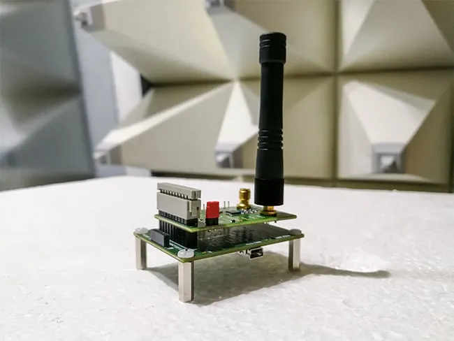
Shielding effectiveness is confirmed on the finished assembly, not on the bare board. We expect the customer to measure in a semi-anechoic chamber with the complete sheet-metal enclosure closed; the target is usually 40–60 dB attenuation across the frequency band of interest. If the first samples fall short, the fastest factory-side fix is to increase via density or enlarge the bare-copper contact zones rather than re-spin the entire stack-up.
When the strict edge-contact rules can be relaxed
For boards whose highest intentional frequency sits below 50 MHz and whose enclosure is a simple single-piece deep-drawn can with no removable lid, we sometimes accept a 0.5 mm copper pull-back and fewer vias, provided the mechanical design guarantees continuous pressure along the entire perimeter. Low-volume prototype runs can also trade some shielding margin for faster turnaround by omitting the soldermask openings and relying on screw pressure alone. Once the product moves to volume or the spectrum content climbs into the hundreds of megahertz, those shortcuts are removed and the full continuous-contact rules are restored. The trade-off is always the same: every millimetre of uncontrolled gap costs shielding effectiveness that cannot be recovered later in software or filtering.