










PCB Specifications
| Parameter | Value | Parameter | Value |
|---|---|---|---|
| PCB Type | Aluminum PCB | Quantity | 20 pcs |
| Layers | 2 Layers | Board Type | Panel PCB |
| Dimensions | 121 x 176.5 mm | Copper Weight | 2oz |
| Thickness | 3 mm | Min Track / Spacing | 10/10mil |
| Surface Finish | OSP | Min Hole Size | 1.0mm |
| Solder Mask | White | Silkscreen | Black |
| Thermal Conductivity | 2.0W | Voltage Withstand | AC2500V |
Manufacturing Timeline
Logistics Information
Key Manufacturing Processes
Manufacturing Summary
This order comprised 20 aluminum PCBs produced in panel format, each with a 3 mm thick core offering 2.0 W/mK thermal conductivity for effective heat spreading. The 2-layer boards measured 121 × 176.5 mm overall, utilized 2 oz copper, maintained 10/10 mil track and spacing, 1.0 mm minimum holes, and satisfied AC 2500 V withstand requirements. White solder mask, black silkscreen, and OSP surface finish were selected to preserve thermal performance while ensuring clear assembly contrast.
Metal base preparation and thermal insulation lamination were performed first to establish stable dielectric layers between the aluminum substrate and circuit planes. Controlled copper electroplating and etching produced uniform 2 oz traces, followed by solder mask application, organic coating, and anti-oxidation treatment calibrated specifically for the OSP aluminum PCB surface. Heat dissipation paths received particular attention during lamination and final profiling.
Electrical testing verified voltage withstand, continuity, and isolation across all 20 panels. The 20.1-day production window allowed measured pacing of each process, resulting in consistent thermal and mechanical properties suited to high-power assemblies.
Explore More PCB Manufacturing Resources
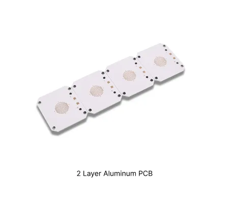
2 Layer Aluminum PCB Manufacturing Insights
These PCBs feature two copper layers on an aluminum substrate with thin dielectric for thermal transfer. They support higher circuit density than single layer designs while maintaining superior heat dissipation.
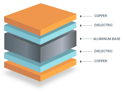
Engineering Challenges in 2 Layer Aluminum PCB Manufacturing: DFM and Thermal Issues
Explore common engineering queries in 2 layer aluminum PCB manufacturing, including CTE mismatch, thermal via design, dielectric bonding, and solder mask registration issues. Learn practical DFM solutions to reduce warpage, improve thermal performance, and increase production yield.
Real Production Records
| Order ID | PCB Type | Layers | Dimensions | Solder Mask | Surface Finish | Quantity | Action |
|---|---|---|---|---|---|---|---|
| ALU-20260727-042 | Aluminum PCB | 2 | 30.1 x 49.91 | White | HASL Lead Free | 120 | View detail |
| ALU-20260511-016 | Aluminum PCB | 2 | 91 x 70 | Green | ENIG (Immersion Gold) | 10 | View detail |
| ALU-20260411-047 | Aluminum PCB | 2 | 102 x 227 | White | ENIG (Immersion Gold) | 10 | View detail |


