










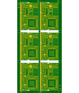
PCB Specifications
| Parameter | Value | Parameter | Value |
|---|---|---|---|
| PCB Type | FR4 PCB | Quantity | 30 pcs |
| Layers | 8 Layers | Board Type | Panel PCB |
| Dimensions | 226.8 x 109 mm | Copper Weight | 1oz |
| Thickness | 1 mm | Min Track / Spacing | 4/4mil |
| Surface Finish | ENIG (Immersion Gold) | Min Hole Size | 0.2mm |
| Solder Mask | Green | Silkscreen | White |
| Stack-up | Custom | Impedance Control | No |
Manufacturing Timeline
Logistics Information
Key Manufacturing Processes
Manufacturing Summary
This production record covers 30 panels of 8-layer PCBs measuring 226.8 × 109 mm with 1.0 mm finished thickness and 1 oz copper weight. The design specified a tighter 4/4 mil trace and spacing geometry together with 0.2 mm minimum holes, supported by a custom stackup that compressed eight layers into the target thickness while maintaining registration across the panel format.
Manufacturing began with engineering review of the stackup, followed by inner layer imaging, circuit etching, and high-pressure lamination to secure layer alignment. Green soldermask and white silkscreen were applied prior to electroless nickel and immersion gold deposition, producing a flat, oxidation-resistant ENIG surface suited to the fine-pitch layout and assembly requirements.
Full electrical testing verified continuity and isolation on every panel. The complete sequence, executed without deviation from the defined process parameters, required 12.3 days and delivered boards exhibiting consistent edge definition, plating uniformity, and solder mask registration.
Explore More PCB Manufacturing Resources
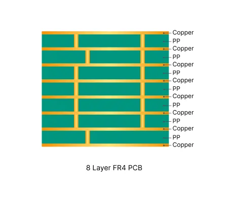
8 Layer FR4 PCB Manufacturing Insights
Discover how AIVON manufactures 8 Layer FR4 PCBs, including advanced multilayer structures, signal integrity requirements, impedance control, fabrication processes, manufacturing challenges, and real production experience from customer orders.

How to Avoid Common Engineering Queries in Multilayer FR4 PCB Design
Real multilayer FR4 PCB CAM review cases covering stack-up confirmation, impedance control, copper balance, via tenting, and edge clearance EQs. Discover practical DFM best practices for 4-layer and higher boards to reduce engineering queries, prevent warpage, and improve first-pass yield.
Real Production Records
| Order ID | PCB Type | Layers | Dimensions | Solder Mask | Surface Finish | Quantity | Action |
|---|---|---|---|---|---|---|---|
| FR4-20260819-043 | FR4 PCB | 10 | 157 x 140 | Blue | ENIG (Immersion Gold) | 100 | View detail |
| FR4-20260818-014 | FR4 PCB | 2 | 110.32 x 173.3 | Green | ENIG (Immersion Gold) | 200 | View detail |
| FR4-20260811-033 | FR4 PCB | 8 | 226.8 x 10⁹ | Green | ENIG (Immersion Gold) | 50 | View detail |


