










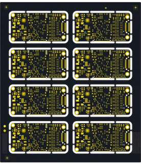
PCB Specifications
| Parameter | Value | Parameter | Value |
|---|---|---|---|
| PCB Type | FR4 PCB | Quantity | 20 pcs |
| Layers | 8 Layers | Board Type | Panel PCB |
| Dimensions | 179 x 157 mm | Copper Weight | 1oz |
| Thickness | 1.6 mm | Min Track / Spacing | 4/4mil |
| Surface Finish | ENIG (Immersion Gold) | Min Hole Size | 0.2mm |
| Solder Mask | Black | Silkscreen | White |
| Stack-up | Custom | Impedance Control | No |
Manufacturing Timeline
Logistics Information
Key Manufacturing Processes
Manufacturing Summary
These 8-layer FR4 PCBs were produced as 20 panels measuring 179 x 157 mm at 1.6 mm thickness with 1 oz copper. The design included blind vias, a custom stackup, and 4/4 mil minimum track spacing, requiring precise inner layer imaging, etching, and registration control to maintain feature accuracy across all layers. Material preparation emphasized clean foil surfaces and stable prepreg to support the 0.2 mm minimum holes without compromising plating quality.
Layer stack alignment and high-pressure lamination bonded the eight layers reliably before black soldermask and white silkscreen application. Electroless nickel deposition followed by immersion gold created a uniform ENIG surface finish, delivering flat pads and good oxidation resistance suited to the board complexity. The full sequence concluded with comprehensive electrical testing that verified continuity and isolation on every panel.
The 23-day production window permitted methodical execution of each process step, resulting in consistent via formation, copper distribution, and solder mask registration. All boards met the specified parameters with no rework required, providing the customer with dependable multilayer panels ready for assembly.
Explore More PCB Manufacturing Resources
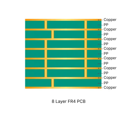
8 Layer FR4 PCB Manufacturing Insights
Discover how AIVON manufactures 8 Layer FR4 PCBs, including advanced multilayer structures, signal integrity requirements, impedance control, fabrication processes, manufacturing challenges, and real production experience from customer orders.

How to Avoid Common Engineering Queries in Multilayer FR4 PCB Design
Real multilayer FR4 PCB CAM review cases covering stack-up confirmation, impedance control, copper balance, via tenting, and edge clearance EQs. Discover practical DFM best practices for 4-layer and higher boards to reduce engineering queries, prevent warpage, and improve first-pass yield.
Real Production Records
| Order ID | PCB Type | Layers | Dimensions | Solder Mask | Surface Finish | Quantity | Action |
|---|---|---|---|---|---|---|---|
| FR4-20260819-043 | FR4 PCB | 10 | 157 x 140 | Blue | ENIG (Immersion Gold) | 100 | View detail |
| FR4-20260818-014 | FR4 PCB | 2 | 110.32 x 173.3 | Green | ENIG (Immersion Gold) | 200 | View detail |
| FR4-20260811-033 | FR4 PCB | 8 | 226.8 x 10⁹ | Green | ENIG (Immersion Gold) | 50 | View detail |


