










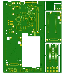
PCB Specifications
| Parameter | Value | Parameter | Value |
|---|---|---|---|
| PCB Type | HDI PCB | Quantity | 10 pcs |
| Layers | 8 Layers | Board Type | Single PCB |
| Dimensions | 198 x 163 mm | Copper Weight | 1oz |
| Thickness | 1.6 mm | Min Track / Spacing | 3/3mil |
| Surface Finish | ENIG (Immersion Gold) | Min Hole Size | 0.25mm |
| Solder Mask | Green | Silkscreen | None |
| HDI Structure | 2 | Blind/Buried Vias | No |
Manufacturing Timeline
Logistics Information
Key Manufacturing Processes
Manufacturing Summary
This 8-layer HDI PCB order, quantity 10 pieces at 198 × 163 mm and 1.6 mm thickness, featured a 2-structure HDI build with 3/3 mil minimum track/spacing, 1 oz copper, 0.25 mm minimum holes, green solder mask, and ENIG finish. No silkscreen was specified. Key process attention centered on precise hole attribute definition and outer-layer pad consistency, because several indicated holes required plating yet showed incomplete or undersized annular rings relative to the drill size, while selected inner layers carried network connections. Where plating was retained, pads were adjusted to maintain adequate copper coverage; where non-plated treatment was confirmed, pads were enlarged by 0.3 mm on one side with corresponding solder-mask openings to avoid reliability risk at the via interfaces.
Additional DFM points included pad-to-pad gaps below 5 mil that would have eliminated solder-mask bridges; the pads were selectively trimmed to preserve bridges without compromising electrical clearance. Window openings that differed from actual pad geometry were realigned to the original copper footprints. Because the board carried no legend, the production serial number was applied as a windowed feature on the bottom solder-mask layer across all four design variants. Original bottom-layer positive text was evaluated for orientation and left unmirrored after confirmation. Panelization used bridge connections rather than stamp holes, as the connecting ribs were too narrow to accept them. Gold-finger pads received window treatment matching the supplied drawing style. These controlled adjustments, consistent with established HDI hole attribute and solder mask bridge control practice, produced boards meeting the tighter geometry and surface-finish requirements with stable registration and reliable delivery.
Explore More PCB Manufacturing Resources
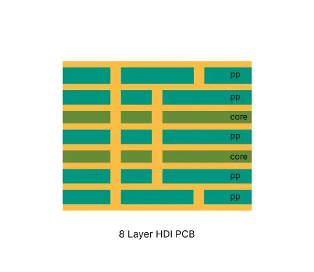
8 Layer HDI PCB Manufacturing Insights
Discover how AIVON manufactures 8 Layer HDI PCBs, including high-density interconnect structures, complex stackup management, microvia reliability, manufacturing challenges, and real production experience from customer orders.
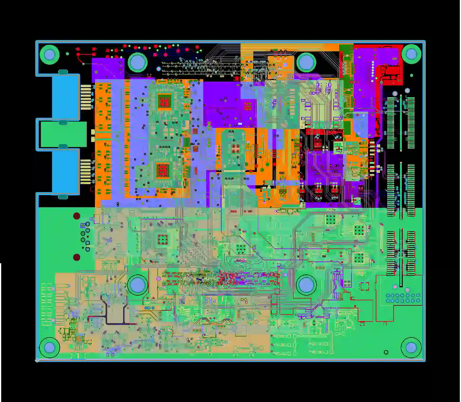
Multilayer HDI PCB Common Engineering Queries in Manufacturing
Multilayer HDI PCBs frequently trigger CAM EQs on microvia spacing, via-in-pad plugging, stack-up, and impedance. Learn real root causes and design rules that raise first-pass yield.
Real Production Records
| Order ID | PCB Type | Layers | Dimensions | Solder Mask | Surface Finish | Quantity | Action |
|---|---|---|---|---|---|---|---|
| HDI-20260729-036 | HDI PCB | 8 | 97 x 93.4 | Black | ENIG (Immersion Gold) | 100 | View detail |
| HDI-20260720-0001 | HDI PCB | 8 | 188 x 100 | Matte Black | ENIG (Immersion Gold) | 125 | View detail |
| HDI-20260718-0002 | HDI PCB | 4 | 37 x 26.6 | Green | ENIG (Immersion Gold) | 20 | View detail |


