










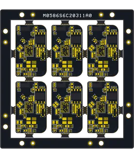
PCB Specifications
| Parameter | Value | Parameter | Value |
|---|---|---|---|
| PCB Type | HDI PCB | Quantity | 30 pcs |
| Layers | 6 Layers | Board Type | Panel PCB |
| Dimensions | 23.7 x 14.4 mm | Copper Weight | 1oz |
| Thickness | 0.8 mm | Min Track / Spacing | 4/4mil |
| Surface Finish | ENIG (Immersion Gold) | Min Hole Size | 0.1mm |
| Solder Mask | Black | Silkscreen | White |
| HDI Structure | 1 | Blind/Buried Vias | Yes |
Manufacturing Timeline
Logistics Information
Key Manufacturing Processes
Manufacturing Summary
The production record for this High-Density Interconnect PCB order covered 30 panels built to 6 layers with blind vias in a 1+n+1 configuration. At 0.8 mm finished thickness and with overall panel dimensions of 23.7 by 14.4 mm, the design incorporated 4/4 mil minimum track and spacing as well as 0.1 mm laser-drilled holes. These parameters required sequential lamination after the initial laser microvia drilling and plating steps.
We prepared the materials and performed precise layer stack alignment prior to high-pressure lamination to maintain the tight registration needed for this geometry. Following circuit formation, black soldermask and white legend were applied before the electroless nickel and immersion gold deposition. Electrical testing at the end confirmed that all 30 panels met the design criteria for continuity and isolation.
The complete manufacturing cycle took 17.4 days from initial engineering review through final inspection. This execution highlights the process controls applied to produce consistent HDI PCBs with ENIG finish for reliable downstream assembly.
Explore More PCB Manufacturing Resources
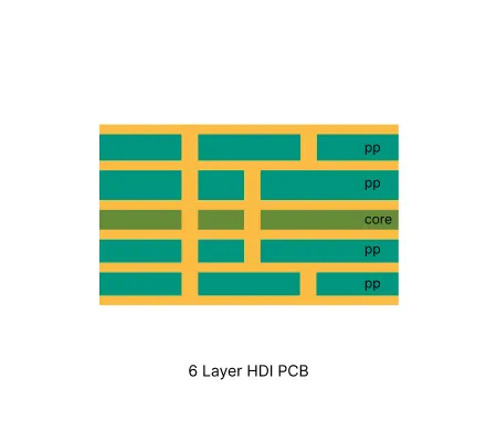
6 Layer HDI PCB Manufacturing Insights
Discover how AIVON manufactures 6 Layer HDI PCBs, including advanced microvia technology, multilayer interconnection control, sequential lamination processes, manufacturing challenges, and real production experience from customer orders.
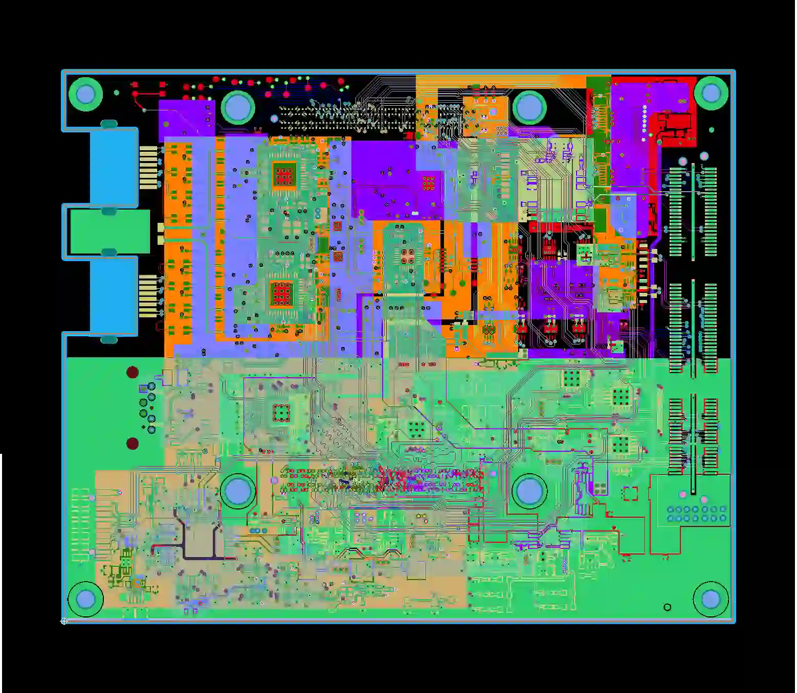
Multilayer HDI PCB Common Engineering Queries in Manufacturing
Multilayer HDI PCBs frequently trigger CAM EQs on microvia spacing, via-in-pad plugging, stack-up, and impedance. Learn real root causes and design rules that raise first-pass yield.
Real Production Records
| Order ID | PCB Type | Layers | Dimensions | Solder Mask | Surface Finish | Quantity | Action |
|---|---|---|---|---|---|---|---|
| HDI-20260729-036 | HDI PCB | 8 | 97 x 93.4 | Black | ENIG (Immersion Gold) | 100 | View detail |
| HDI-20260720-0001 | HDI PCB | 8 | 188 x 100 | Matte Black | ENIG (Immersion Gold) | 125 | View detail |
| HDI-20260718-0002 | HDI PCB | 4 | 37 x 26.6 | Green | ENIG (Immersion Gold) | 20 | View detail |


