










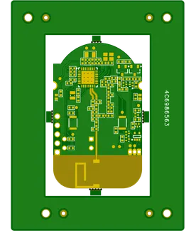
PCB Specifications
| Parameter | Value | Parameter | Value |
|---|---|---|---|
| PCB Type | HDI PCB | Quantity | 10 pcs |
| Layers | 4 Layers | Board Type | Panel PCB |
| Dimensions | 41.4 x 25.4 mm | Copper Weight | 1oz |
| Thickness | 1.6 mm | Min Track / Spacing | 6/6mil↑ |
| Surface Finish | ENIG (Immersion Gold) | Min Hole Size | 0.2mm |
| Solder Mask | Green | Silkscreen | White |
| HDI Structure | 1 | Blind/Buried Vias | Yes |
Manufacturing Timeline
Logistics Information
Key Manufacturing Processes
Manufacturing Summary
This 4-layer HDI panel PCB order consisted of 10 boards measuring 41.4 × 25.4 mm with 1.6 mm thickness and 1 oz copper layers. The design specified blind vias in a 1-step HDI structure, which we addressed through sequential lamination and laser microvia drilling. Via filling and plating were completed immediately afterward to secure reliable interconnections before moving to solder mask application.
A 6/6 mil trace and spacing requirement aligned with standard geometry, enabling conventional inner layer imaging and etching while we maintained tight layer-to-layer registration. Green soldermask, white silkscreen, and immersion gold ENIG surface finish were applied to support assembly needs and long-term pad integrity. The full sequence—from material preparation through electroless nickel and immersion gold deposition—concluded with 100% electrical testing.
The 12-day production run delivered uniform results across the batch, confirming consistent via plating and lamination quality for this HDI configuration.
Explore More PCB Manufacturing Resources
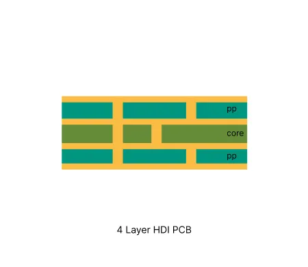
4 Layer HDI PCB Manufacturing Insights
Discover how AIVON manufactures 4 Layer HDI PCBs, including microvia structures, fine-line routing requirements, sequential lamination processes, manufacturing challenges, and real production experience from customer orders.
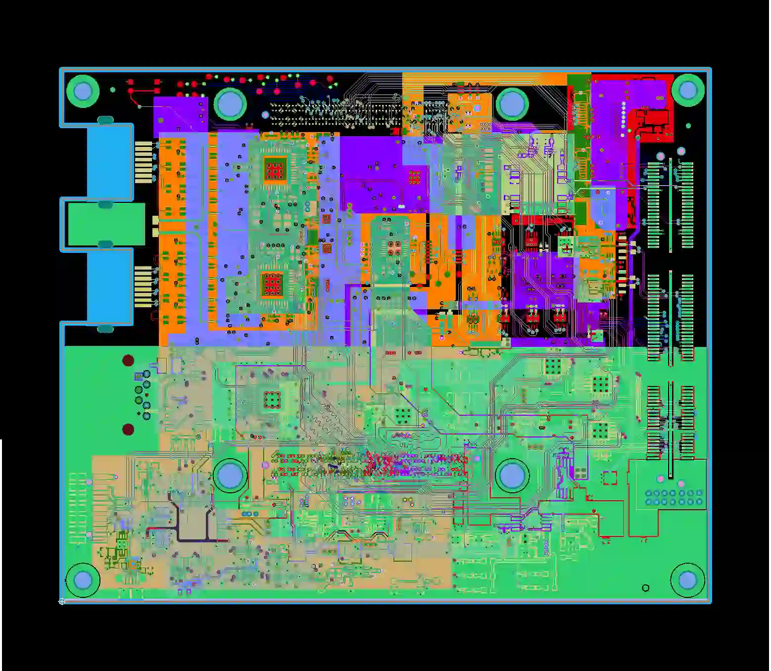
Multilayer HDI PCB Common Engineering Queries in Manufacturing
Multilayer HDI PCBs frequently trigger CAM EQs on microvia spacing, via-in-pad plugging, stack-up, and impedance. Learn real root causes and design rules that raise first-pass yield.
Real Production Records
| Order ID | PCB Type | Layers | Dimensions | Solder Mask | Surface Finish | Quantity | Action |
|---|---|---|---|---|---|---|---|
| HDI-20260729-036 | HDI PCB | 8 | 97 x 93.4 | Black | ENIG (Immersion Gold) | 100 | View detail |
| HDI-20260720-0001 | HDI PCB | 8 | 188 x 100 | Matte Black | ENIG (Immersion Gold) | 125 | View detail |
| HDI-20260718-0002 | HDI PCB | 4 | 37 x 26.6 | Green | ENIG (Immersion Gold) | 20 | View detail |


