










PCB Specifications
| Parameter | Value | Parameter | Value |
|---|---|---|---|
| PCB Type | HDI PCB | Quantity | 225 pcs |
| Layers | 8 Layers | Board Type | Panel PCB |
| Dimensions | 22 x 32.5 mm | Copper Weight | 1oz |
| Thickness | 0.8 mm | Min Track / Spacing | 4/4mil |
| Surface Finish | ENIG (Immersion Gold) | Min Hole Size | 0.1mm |
| Solder Mask | Green | Silkscreen | White |
| Stack-up | Custom | Impedance Control | No |
| HDI Structure | 1 | Blind/Buried Vias | Yes |
Manufacturing Timeline
Logistics Information
Key Manufacturing Processes
Manufacturing Summary
This 8-layer HDI PCB order was produced at 0.8 mm finished thickness with mixed copper weights, ultimately executed as 1 oz inner layers and 1 oz outer layers after DFM review. The board size of 22 × 32.5 mm, 0.1 mm minimum hole size, and 4 mil minimum trace/space presented tight geometry for an 8-layer stackup. Panelization used a single-image step-and-repeat layout with bridging and stamp holes to optimize material utilization and downstream assembly handling for the 225-piece (15-set) quantity.
Key DFM challenges included insufficient inner-layer copper-to-copper spacing for the originally requested 2 oz inner copper weight, which would have compromised etching yield and reliability at 4 mil features. The design was adjusted to 1 oz inner layers with corresponding lamination parameters to achieve 0.89 mm ± 0.1 mm pressed thickness while maintaining impedance-neutral performance. Edge clearance concerns on multiple pads (under 0.2 mm to board edge) were resolved through controlled routing and solder mask opening adjustments to prevent excessive copper exposure without affecting functional pad integrity. Solder mask alignment and silkscreen (top-side white only) were verified against the optimized stencil data.
Production proceeded with standard ENIG surface finish and 100% flying probe testing. All engineering changes were implemented and documented prior to release, ensuring consistent delivery within the 14-day window. Detailed resolution of the copper weight and edge clearance adjustments for this panelization scheme is available in the engineering case study.
Explore More PCB Manufacturing Resources
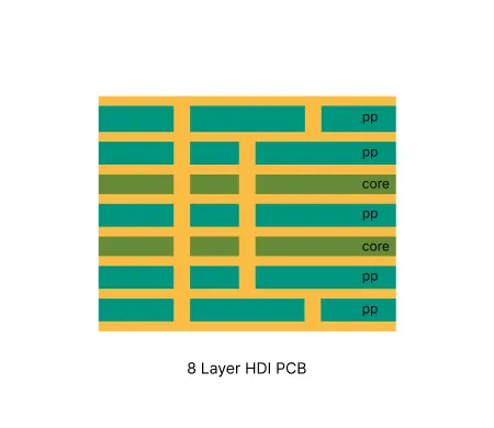
8 Layer HDI PCB Manufacturing Insights
Discover how AIVON manufactures 8 Layer HDI PCBs, including high-density interconnect structures, complex stackup management, microvia reliability, manufacturing challenges, and real production experience from customer orders.
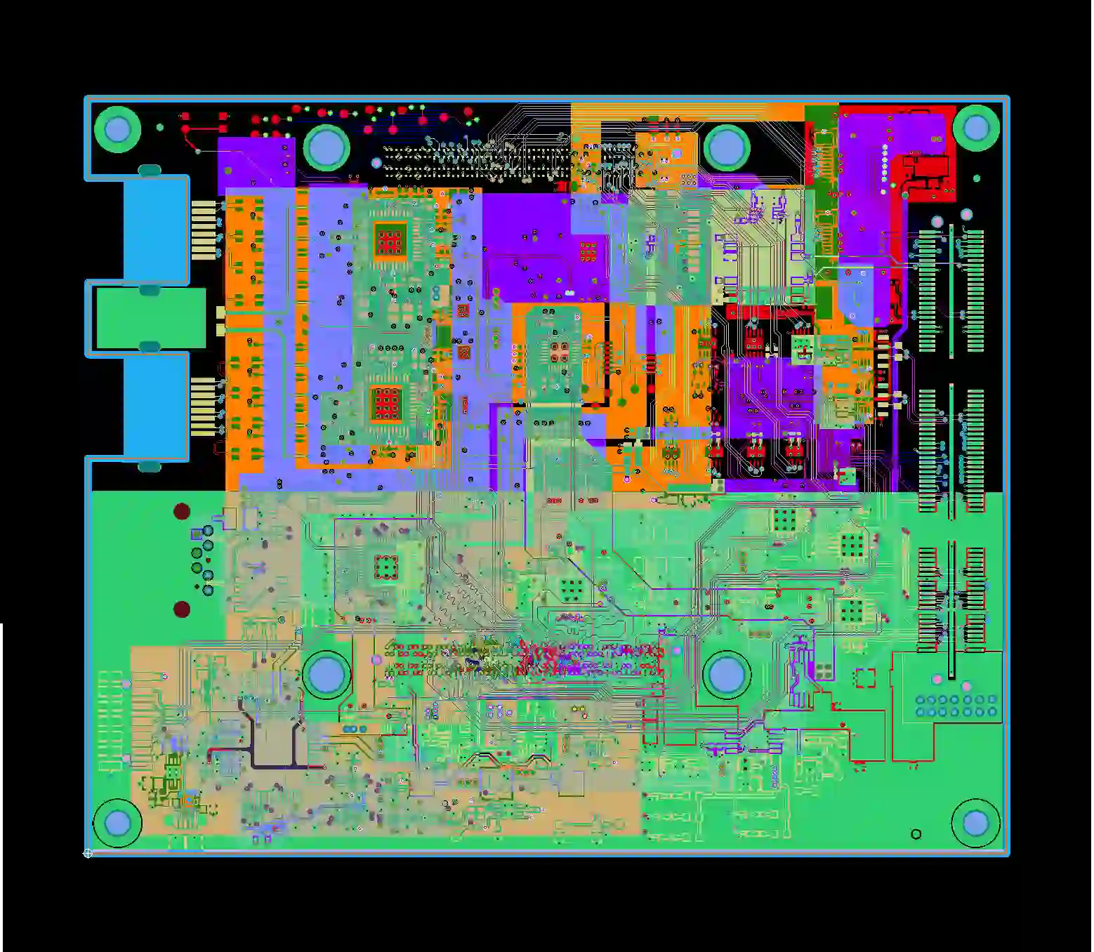
Multilayer HDI PCB Common Engineering Queries in Manufacturing
Multilayer HDI PCBs frequently trigger CAM EQs on microvia spacing, via-in-pad plugging, stack-up, and impedance. Learn real root causes and design rules that raise first-pass yield.
Real Production Records
| Order ID | PCB Type | Layers | Dimensions | Solder Mask | Surface Finish | Quantity | Action |
|---|---|---|---|---|---|---|---|
| HDI-20260729-036 | HDI PCB | 8 | 97 x 93.4 | Black | ENIG (Immersion Gold) | 100 | View detail |
| HDI-20260720-0001 | HDI PCB | 8 | 188 x 100 | Matte Black | ENIG (Immersion Gold) | 125 | View detail |
| HDI-20260718-0002 | HDI PCB | 4 | 37 x 26.6 | Green | ENIG (Immersion Gold) | 20 | View detail |


