










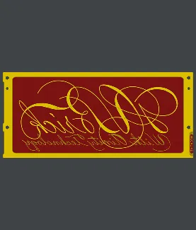
PCB Specifications
| Parameter | Value | Parameter | Value |
|---|---|---|---|
| PCB Type | HDI PCB | Quantity | 20 pcs |
| Layers | 4 Layers | Board Type | Single PCB |
| Dimensions | 162 x 73 mm | Copper Weight | 1oz |
| Thickness | 1.6 mm | Min Track / Spacing | 4/4mil |
| Surface Finish | ENIG (Immersion Gold) | Min Hole Size | 0.15mm |
| Solder Mask | Red | Silkscreen | White |
Manufacturing Timeline
Logistics Information
Key Manufacturing Processes
Manufacturing Summary
This 4-layer HDI PCB was produced in a batch of 20 pieces (162 × 73 mm boards) using Shengyi material at 1.6 mm nominal thickness and 1 oz copper on both inner and outer layers. Key process parameters included 0.15 mm minimum hole size, 4 mil trace/space geometry, ENIG surface finish, and mechanical forming. The design required careful registration control for four countersink holes placed on copper features, with target depths calculated at 1.35 mm to maintain structural integrity and assembly fit. 100% flying probe testing and electrical performance reports were completed before shipment within the 13-day delivery window.
Engineering review identified inconsistencies between the customer-provided stackup and available core materials. The original 1.5 mm copper-free core was unavailable from standard inventory, leading to evaluation of 1.53 mm and 1.43 mm alternatives. Board thickness was adjusted to 1.8 mm ±10% after confirmation, while preserving overall impedance and mechanical targets. Countersink depth calculations and copper-hole integration were verified through multiple iterations to avoid plating or depth control issues during drilling. These stackup deviation and countersink adjustments were resolved by updating the lamination parameters and confirming the revised structure with the customer prior to release.
Production proceeded smoothly after final DFM confirmation, with no major defects observed in plating, etching, or hole quality. The completed boards met all dimensional and electrical requirements, demonstrating consistent results despite the material substitution and precision hole features. Full quality documentation including test reports and certificate of conformity accompanied the shipment.
Explore More PCB Manufacturing Resources
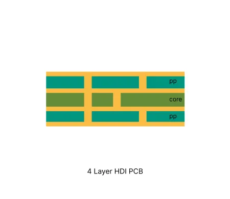
4 Layer HDI PCB Manufacturing Insights
These boards deliver high routing density through laser-drilled microvias and sequential lamination while maintaining controlled production costs.
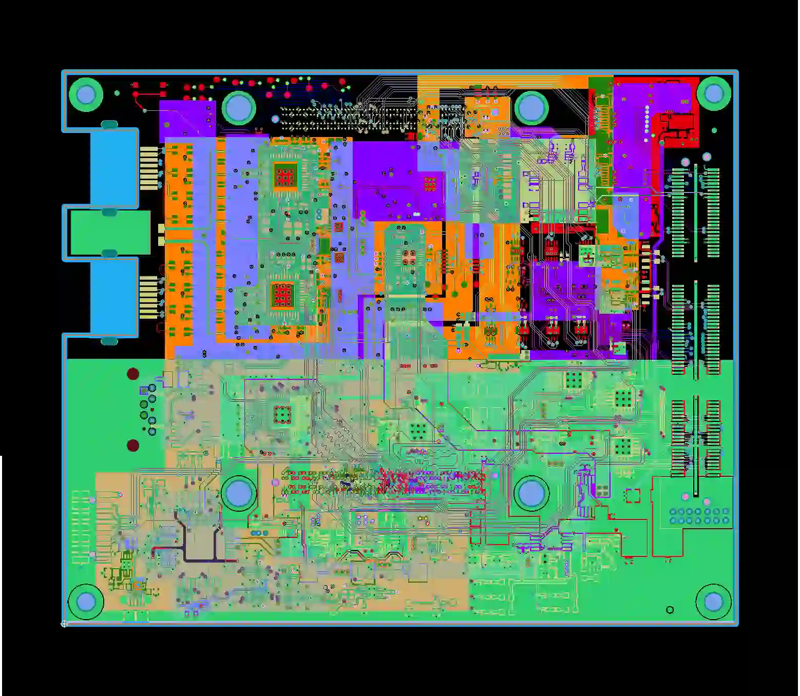
Multilayer HDI PCB Common Engineering Queries in Manufacturing
Senior PCB manufacturing engineer shares real factory insights on common engineering queries for multilayer HDI PCBs including 4 Layer HDI PCB, 6 Layer HDI PCB, 8 Layer HDI PCB, and 10 Layer HDI PCB. Learn about microvia stacking, registration challenges, impedance control, and practical DFM tips to reduce EQs and improve production yield.
Real Production Records
| Order ID | PCB Type | Layers | Dimensions | Solder Mask | Surface Finish | Quantity | Action |
|---|---|---|---|---|---|---|---|
| HDI-20260729-036 | HDI PCB | 8 | 97 x 93.4 | Black | ENIG (Immersion Gold) | 100 | View detail |
| HDI-20260720-0001 | HDI PCB | 8 | 188 x 100 | Matte Black | ENIG (Immersion Gold) | 125 | View detail |
| HDI-20260718-0002 | HDI PCB | 4 | 37 x 26.6 | Green | ENIG (Immersion Gold) | 20 | View detail |


