










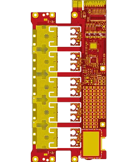
PCB Specifications
| Parameter | Value | Parameter | Value |
|---|---|---|---|
| PCB Type | HDI PCB | Quantity | 20 pcs |
| Layers | 6 Layers | Board Type | Single PCB |
| Dimensions | 81 x 173 mm | Copper Weight | 2oz |
| Thickness | 1.6 mm | Min Track / Spacing | 6/6mil↑ |
| Surface Finish | ENIG (Immersion Gold) | Min Hole Size | 0.3mm↑ |
| Solder Mask | Red | Silkscreen | White |
| HDI Structure | 1 | Blind/Buried Vias | Yes |
Manufacturing Timeline
Logistics Information
Key Manufacturing Processes
Manufacturing Summary
This production run of 20 boards delivered a 6-layer HDI PCB featuring blind microvias in a 1-step structure. The 81 × 173 mm panels at 1.6 mm thickness carried 2 oz copper on all layers, calling for sequential lamination after laser microvia drilling and subsequent via filling to maintain reliable layer-to-layer connections. Material preparation and stack alignment received close attention to control registration across the thicker copper foils.
Red soldermask and white silkscreen were applied with uniform coverage before the immersion gold ENIG surface finish, chosen to ensure flat pad topography and robust solder joint formation. Although the 6/6 mil trace and spacing stayed within conventional parameters, the combination of HDI geometry, 2 oz copper, and controlled etching required precise plating and etch compensation to preserve trace profiles and electrical performance.
Electrical testing of all 20 boards confirmed continuity and isolation across the blind via network. The complete cycle from engineering review through final inspection spanned 15.2 days, resulting in consistent dimensional and electrical outcomes for this HDI PCB order.
Explore More PCB Manufacturing Resources
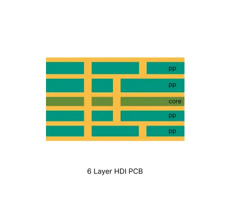
6 Layer HDI PCB Manufacturing Insights
This page details production methods, specification ranges, and optimization techniques for reliable 6 layer HDI circuit boards.
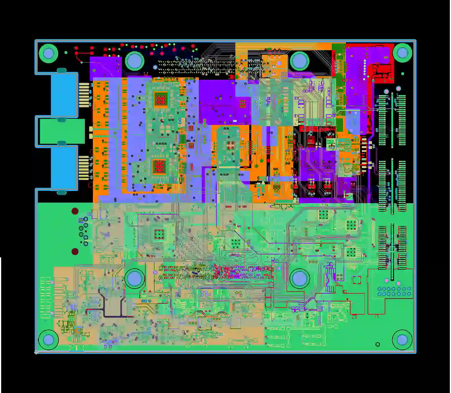
Multilayer HDI PCB Common Engineering Queries in Manufacturing
Senior PCB manufacturing engineer shares real factory insights on common engineering queries for multilayer HDI PCBs including 4 Layer HDI PCB, 6 Layer HDI PCB, 8 Layer HDI PCB, and 10 Layer HDI PCB. Learn about microvia stacking, registration challenges, impedance control, and practical DFM tips to reduce EQs and improve production yield.
Real Production Records
| Order ID | PCB Type | Layers | Dimensions | Solder Mask | Surface Finish | Quantity | Action |
|---|---|---|---|---|---|---|---|
| HDI-20260729-036 | HDI PCB | 8 | 97 x 93.4 | Black | ENIG (Immersion Gold) | 100 | View detail |
| HDI-20260720-0001 | HDI PCB | 8 | 188 x 100 | Matte Black | ENIG (Immersion Gold) | 125 | View detail |
| HDI-20260718-0002 | HDI PCB | 4 | 37 x 26.6 | Green | ENIG (Immersion Gold) | 20 | View detail |


