










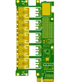
PCB Specifications
| Parameter | Value | Parameter | Value |
|---|---|---|---|
| PCB Type | HDI PCB | Quantity | 20 pcs |
| Layers | 6 Layers | Board Type | Single PCB |
| Dimensions | 81 x 173 mm | Copper Weight | 2oz |
| Thickness | 1.6 mm | Min Track / Spacing | 6/6mil↑ |
| Surface Finish | ENIG (Immersion Gold) | Min Hole Size | 0.3mm↑ |
| Solder Mask | Matte Green | Silkscreen | White |
| HDI Structure | 1 | Blind/Buried Vias | Yes |
Manufacturing Timeline
Logistics Information
Key Manufacturing Processes
Manufacturing Summary
Twenty single 6-layer HDI PCBs with blind vias were produced for this order, each measuring 81 by 173 mm and built to 1.6 mm thickness using 2 oz copper throughout. Sequential lamination and laser microvia drilling established the blind via connections in the specified structure, after which via filling, plating, and thick copper electroplating were performed to support the heavier copper while meeting the 6/6 mil minimum trace and spacing. These steps required exact control during material preparation and circuit imaging to prevent over-etching on the outer layers.
Matte green solder mask and white silkscreen were applied prior to immersion gold ENIG surface finish, delivering good contrast and reliable pad protection. High-pressure lamination together with precise layer stack alignment maintained registration across the build, and controlled copper etching preserved feature definition on all layers. The chosen processes directly addressed the demands of the HDI construction and 2 oz copper without introducing unnecessary complexity.
Final electrical testing verified continuity, isolation, and via integrity on every board, confirming consistent results across the batch of 20. Execution followed the full sequence from engineering review through electroless nickel and immersion gold deposition, producing boards that match the supplied specifications in both geometry and reliability.
Explore More PCB Manufacturing Resources
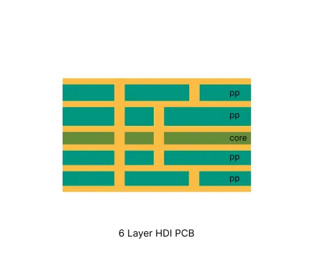
6 Layer HDI PCB Manufacturing Insights
This page details production methods, specification ranges, and optimization techniques for reliable 6 layer HDI circuit boards.
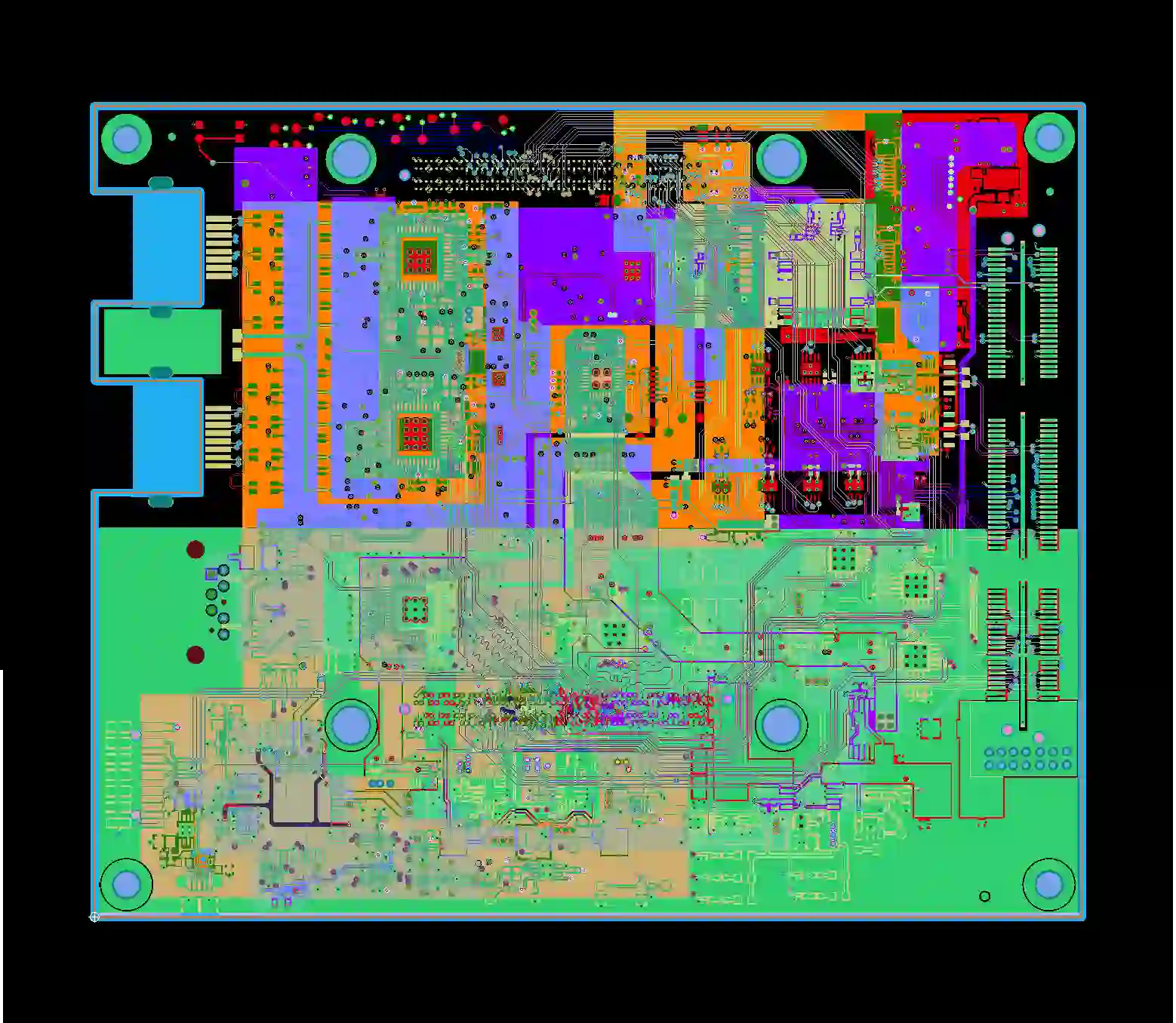
Multilayer HDI PCB Common Engineering Queries in Manufacturing
Senior PCB manufacturing engineer shares real factory insights on common engineering queries for multilayer HDI PCBs including 4 Layer HDI PCB, 6 Layer HDI PCB, 8 Layer HDI PCB, and 10 Layer HDI PCB. Learn about microvia stacking, registration challenges, impedance control, and practical DFM tips to reduce EQs and improve production yield.
Real Production Records
| Order ID | PCB Type | Layers | Dimensions | Solder Mask | Surface Finish | Quantity | Action |
|---|---|---|---|---|---|---|---|
| HDI-20260729-036 | HDI PCB | 8 | 97 x 93.4 | Black | ENIG (Immersion Gold) | 100 | View detail |
| HDI-20260720-0001 | HDI PCB | 8 | 188 x 100 | Matte Black | ENIG (Immersion Gold) | 125 | View detail |
| HDI-20260718-0002 | HDI PCB | 4 | 37 x 26.6 | Green | ENIG (Immersion Gold) | 20 | View detail |


