










PCB Specifications
| Parameter | Value | Parameter | Value |
|---|---|---|---|
| PCB Type | HDI PCB | Quantity | 250 pcs |
| Layers | 10 Layers | Board Type | Panel PCB |
| Dimensions | 80 x 80 mm | Copper Weight | 1oz |
| Thickness | 1.6 mm | Min Track / Spacing | 4/4mil |
| Surface Finish | ENIG (Immersion Gold) | Min Hole Size | 0.1mm |
| Solder Mask | Green | Silkscreen | White |
| Stack-up | Custom | Impedance Control | No |
| HDI Structure | 1 | Blind/Buried Vias | Yes |
Manufacturing Timeline
Logistics Information
Key Manufacturing Processes
Manufacturing Summary
We manufactured 250 pieces of these 10-layer HDI PCBs in panel format, each board measuring 80 × 80 mm with 1.6 mm thickness and 1 oz copper weight. The design included blind vias, a custom stackup, 4/4 mil minimum track and spacing, and 0.1 mm minimum hole size. These tighter geometries required precise inner layer imaging, circuit etching, and layer stack alignment to maintain registration across all ten layers during high pressure lamination.
Green soldermask and white silkscreen were applied prior to electroless nickel and immersion gold deposition, producing a uniform ENIG surface finish suited for reliable assembly. Each production stage—from material preparation through solder mask application and final electrical testing—was executed according to the specified parameters. Batch AOI inspection verified trace integrity and hole quality on every panel.
The 27.2-day schedule allowed thorough verification at each checkpoint for this moderate-volume run. All delivered panels met the custom stackup and blind via requirements, providing the customer with consistent multilayer boards ready for immediate use.
Explore More PCB Manufacturing Resources
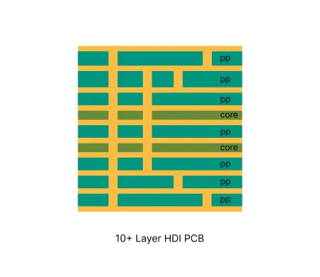
10+ Layer HDI PCB Manufacturing Insights
10+ layer HDI PCBs use sequential lamination and microvia technology to achieve high interconnect density in compact multilayer boards. Supports stacked or staggered microvias with laser-drilled structures. Compatible with high-Tg FR-4 and high-speed laminates.
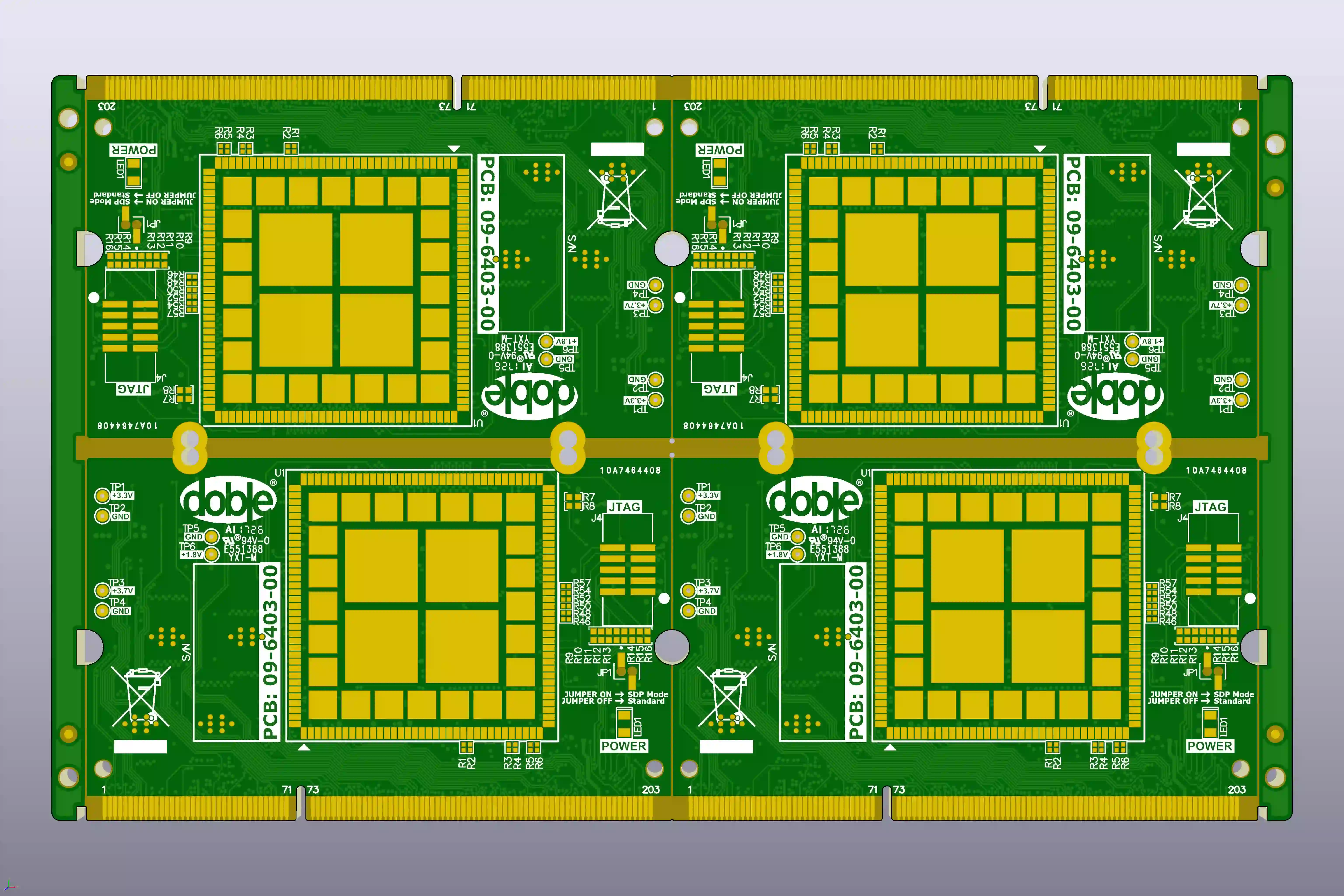
How to Resolve Gold Finger Bevel and Impedance EQs in 10-Layer PCBs
Real 10-layer FR-4 case study: how CAM engineers resolved gold finger bevel clearance, impedance mismatch, tight via spacing and plugging risks to prevent scrap and signal integrity failures.
Real Production Records
| Order ID | PCB Type | Layers | Dimensions | Solder Mask | Surface Finish | Quantity | Action |
|---|---|---|---|---|---|---|---|
| HDI-20260729-036 | HDI PCB | 8 | 97 x 93.4 | Black | ENIG (Immersion Gold) | 100 | View detail |
| HDI-20260720-0001 | HDI PCB | 8 | 188 x 100 | Matte Black | ENIG (Immersion Gold) | 125 | View detail |
| HDI-20260718-0002 | HDI PCB | 4 | 37 x 26.6 | Green | ENIG (Immersion Gold) | 20 | View detail |


