










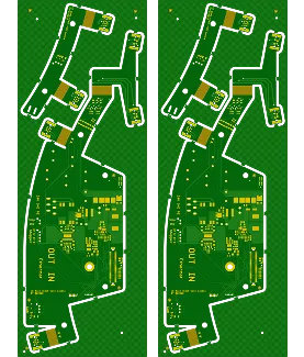
PCB Specifications
| Parameter | Value | Parameter | Value |
|---|---|---|---|
| PCB Type | Rigid-Flex PCB | Quantity | 20 pcs |
| Layers | 4 Layers | Board Type | Panel PCB |
| Dimensions | 106 x 295.5 mm | Copper Weight | 2OZ |
| Thickness | 1.6 mm | Min Track / Spacing | 6/6mil↑ |
| Surface Finish | ENIG (Immersion Gold) | Min Hole Size | 0.3mm↑ |
| Solder Mask | Green | Silkscreen | None |
Manufacturing Timeline
Logistics Information
Key Manufacturing Processes
Manufacturing Summary
This order comprised 20 panels of 4-layer rigid-flex PCB, each measuring 106 × 295.5 mm with 1.6 mm thickness and 2 oz copper weight. The hybrid rigid-flex construction required precise layer stack alignment and flex-rigid lamination to integrate flexible zones without compromising structural stability or introducing stress concentrations. Standard 6/6 mil track spacing and 0.3 mm minimum hole size were maintained throughout, while the heavier copper demanded adjusted etching parameters to preserve trace integrity across both material types.
Inner layer imaging and circuit etching were followed by high-pressure lamination and thick copper electroplating to ensure uniform conductor thickness. Green solder mask was applied before electroless nickel deposition and immersion gold deposition to produce a reliable ENIG finish. Controlled depth routing defined the final panel outlines, respecting the transition areas between rigid and flex sections.
Dynamic flex reliability testing and full electrical testing verified bend endurance and net continuity across the entire batch. The 29.9-day production cycle allowed measured pacing through material preparation, multiple lamination cycles, and quality checkpoints, resulting in consistent boards delivered to specification for this rigid-flex application.
Explore More PCB Manufacturing Resources
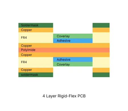
4 Layer Rigid-Flex PCB Manufacturing Insights
Discover how AIVON manufactures 4 Layer Rigid-Flex PCBs, including rigid and flexible layer integration, mechanical reliability requirements, fabrication processes, manufacturing challenges, and real production experience from customer orders.
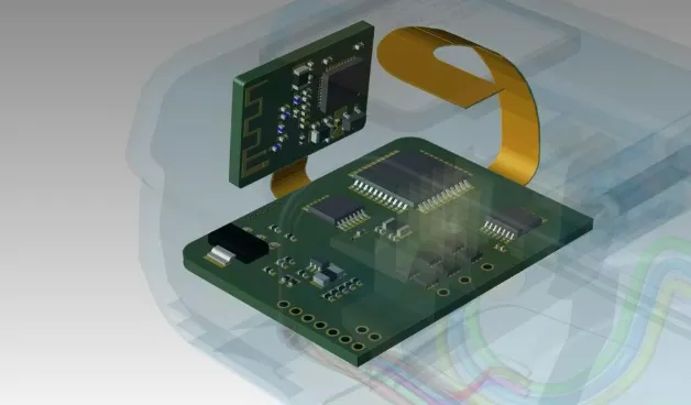
The Ultimate Guide to Rigid-Flex PCB Design: Mastering Reliability, Complexity, and Cost
Master the complexities of Rigid-Flex PCB Design with this 2,500-word guide. Explore stack-up symmetry, bend radius calculations, via optimization, and cost-effective manufacturing strategies.
Real Production Records
| Order ID | PCB Type | Layers | Dimensions | Solder Mask | Surface Finish | Quantity | Action |
|---|---|---|---|---|---|---|---|
| RFP-20260723-038 | Rigid-Flex PCB | 4 | 186 x 111.6 | Green | ENIG (Immersion Gold) | 10 | View detail |
| RFP-20260626-0002 | Rigid-Flex PCB | 4 | 100 x 106.01 | Green | ENIG (Immersion Gold) | 5 | View detail |
| RFP-20260608-0005 | Rigid-Flex PCB | 4 | 22.15 x 97.92 | Green | ENIG (Immersion Gold) | 20 | View detail |


