










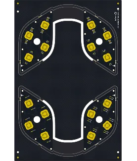
PCB Specifications
| Parameter | Value | Parameter | Value |
|---|---|---|---|
| PCB Type | Rigid-Flex PCB | Quantity | 5 pcs |
| Layers | 4 Layers | Board Type | Panel PCB |
| Dimensions | 180 x 120 mm | Copper Weight | 1OZ |
| Thickness | 1.6 mm | Min Track / Spacing | 6/6mil↑ |
| Surface Finish | ENIG (Immersion Gold) | Min Hole Size | 0.3mm↑ |
| Solder Mask | Black | Silkscreen | White |
Manufacturing Timeline
Logistics Information
Key Manufacturing Processes
Manufacturing Summary
These five panelized 4-layer rigid-flex PCBs measured 180 by 120 mm with 1.6 mm finished thickness and 1 oz copper throughout. The build followed a standard 6/6 mil track and spacing geometry together with 0.3 mm minimum holes, black soldermask, white silkscreen, and immersion gold ENIG surface finish. No blind vias were required, allowing focus on the hybrid stackup where rigid FR4 sections transition into flexible layers.
Production began with detailed engineering review and material preparation matched to the rigid-flex construction. We performed precise layer stack alignment, high pressure lamination, and flex-rigid lamination to ensure stable bonding at the interfaces. Solder mask application preceded electroless nickel and immersion gold deposition, after which controlled depth routing accurately defined the flex regions without damaging adjacent circuitry.
Dynamic flex reliability testing confirmed the panels could endure repeated bending cycles, followed by full electrical testing that showed all boards within specification. The 28-day schedule permitted careful process monitoring for this low-volume order, yielding consistent mechanical and electrical performance suited for end-product integration.
Explore More PCB Manufacturing Resources
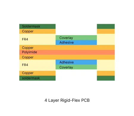
4 Layer Rigid-Flex PCB Manufacturing Insights
Discover how AIVON manufactures 4 Layer Rigid-Flex PCBs, including rigid and flexible layer integration, mechanical reliability requirements, fabrication processes, manufacturing challenges, and real production experience from customer orders.
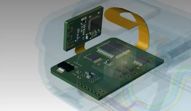
The Ultimate Guide to Rigid-Flex PCB Design: Mastering Reliability, Complexity, and Cost
Master the complexities of Rigid-Flex PCB Design with this 2,500-word guide. Explore stack-up symmetry, bend radius calculations, via optimization, and cost-effective manufacturing strategies.
Real Production Records
| Order ID | PCB Type | Layers | Dimensions | Solder Mask | Surface Finish | Quantity | Action |
|---|---|---|---|---|---|---|---|
| RFP-20260723-038 | Rigid-Flex PCB | 4 | 186 x 111.6 | Green | ENIG (Immersion Gold) | 10 | View detail |
| RFP-20260626-0002 | Rigid-Flex PCB | 4 | 100 x 106.01 | Green | ENIG (Immersion Gold) | 5 | View detail |
| RFP-20260608-0005 | Rigid-Flex PCB | 4 | 22.15 x 97.92 | Green | ENIG (Immersion Gold) | 20 | View detail |


