










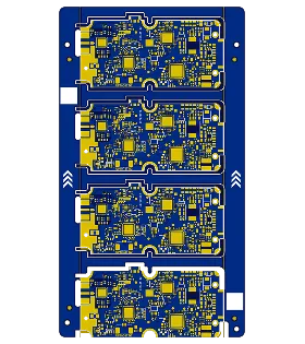
PCB Specifications
| Parameter | Value | Parameter | Value |
|---|---|---|---|
| PCB Type | Rogers PCB | Quantity | 5 pcs |
| Layers | 6 Layers | Board Type | Panel PCB |
| Dimensions | 88 x 156 mm | Copper Weight | 1oz |
| Thickness | 1.2 mm | Min Track / Spacing | 4/4mil |
| Surface Finish | ENIG (Immersion Gold) | Min Hole Size | 0.2mm |
| Solder Mask | Blue | Silkscreen | White |
| Material Type | Rogers/RO4003C |
Manufacturing Timeline
Logistics Information
Key Manufacturing Processes
Manufacturing Summary
This 6-layer Rogers RO4003C PCB order, quantity 5 pieces at 88 × 156 mm and 1.2 mm thickness, used 1 oz copper, 4/4 mil minimum track/spacing, 0.2 mm minimum holes, blue solder mask, white silkscreen, and ENIG finish. The high-frequency material and controlled-impedance requirement made stack-up accuracy and edge integrity primary process points. Calculated impedance values and the corresponding layer stack were submitted for confirmation before lamination, ensuring dielectric consistency across the panel. V-cut centerlines in the original data sat 0.4 mm off the outline, which would have lengthened finished boards by 0.8 mm; the cut paths were realigned to restore nominal dimensions without altering routing clearances.
Several DFM items required direct clarification. A 0.889 mm hole on the top layer lacked a solder-mask opening and would have allowed ink intrusion onto the pad; the opening was added to keep the hole clean. Pads and copper features lying too close to the board edge risked exposed copper after routing; those features were pulled inward or the outline adjusted to eliminate the exposure. Silkscreen characters below 0.2 mm width and 0.76 mm height could not be printed reliably and were enlarged or relocated. Characters placed on large gold areas were reviewed and retained only where functionally required. A line-width conflict between an earlier EQ update (0.317 mm) and the final data set (0.29 mm) was resolved by adopting the latest customer file. Laser-engraved DM-format codes were applied to the four process-edge white-oil blocks as specified. These adjustments, following the same impedance stack-up and edge-copper control approach used on prior high-frequency builds, produced boards that met both the material and electrical targets with consistent registration and on-time delivery.
Explore More PCB Manufacturing Resources
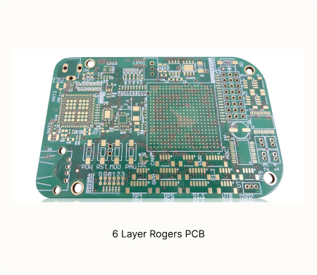
6 Layer Rogers PCB Manufacturing Insights
Discover how AIVON manufactures 6 Layer Rogers PCBs, including complex high-frequency stackup design, advanced material processing, impedance control requirements, manufacturing challenges, and real production experience from customer orders.
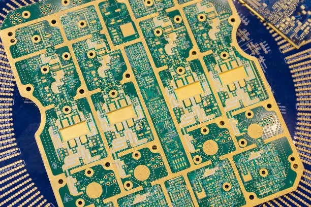
Troubleshooting Common Manufacturing Challenges with Rogers PCBs
Master troubleshooting common Rogers PCB manufacturing challenges including drilling defects, plating adhesion, delamination, and CTE mismatch. Learn practical solutions, process adjustments, and DFM tips to improve yield for high-frequency RO4000, RO4350B, and PTFE-based boards.
Real Production Records
| Order ID | PCB Type | Layers | Dimensions | Solder Mask | Surface Finish | Quantity | Action |
|---|---|---|---|---|---|---|---|
| ROG-20260711-0002 | Rogers PCB | 6 | 86.24 x 60.25 | Green | ENIG (Immersion Gold) | 5 | View detail |
| ROG-20221110-0103 | Rogers PCB | 6 | 73.66 x 50.8 | Green | ENIG (Immersion Gold) | 20 | View detail |
| ROG-20220623-0039 | Rogers PCB | 6 | 50.8 x 73.7 | Green | ENIG (Immersion Gold) | 20 | View detail |


