 00:51
00:51
EMI Shielding
EMI shielding plays a critical role in modern electronics design, protecting sensitive components from electromagnetic interference that can disrupt performance or cause failures. In the context of PCB manufacturing and electronic systems, EMI shielding involves techniques and materials that block or attenuate unwanted electromagnetic radiation, ensuring devices operate reliably in environments filled with signals from wireless networks, power lines, and other sources. This tag, EMI Shielding, gathers articles that delve into the fundamentals of shielding strategies, from basic principles to advanced implementations, helping engineers and hobbyists address common challenges in signal integrity and compliance with standards like FCC or CE regulations. For those searching for EMI shielding solutions, understanding its practical applications is essential. In high-speed PCBs, for instance, shielding can prevent crosstalk between traces or protect against external noise in automotive electronics, medical devices, and telecommunications equipment. Best practices include selecting appropriate shielding materials such as conductive foams, metal enclosures, or copper foil tapes, and integrating them during the design phase to minimize costs and rework. Articles under this tag often highlight actionable insights, like calculating shielding effectiveness using formulas for attenuation or incorporating ground planes and vias to create effective barriers against interference. By exploring the resources here, readers can gain step-by-step guidance on testing EMI levels with tools like spectrum analyzers and implementing fixes such as ferrite beads or gasket seals. Whether you are troubleshooting interference in a prototype or optimizing a production run, these discussions provide the knowledge needed to enhance electromagnetic compatibility and achieve robust, interference-free designs.
Video Guide
-
00:51
Technical Articles
Grounding Fundamentals and Its Critical Role in Electrical and Electronic Systems

Should You Use Solid or Hatched Copper Pour on PCBs?

Inside a Switch-Mode Power Supply: A Component-by-Component Analysis
Classification and Differences of PCB Signal Traces: Microstrip and Stripline
RF PCB Layout and Routing Essentials
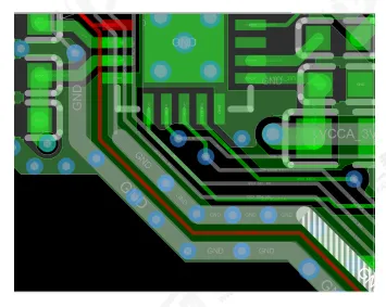
PCB Design Guidelines for Audio Interface Circuits
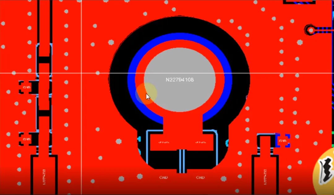
Why Designers Often Tie PCB Ground to Chassis Ground with a Parallel Resistor and Capacitor
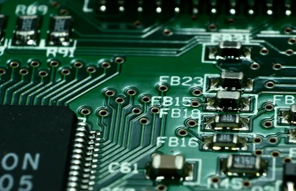
Maintaining PCB Signal Integrity in Harsh Environments: Challenges and Practical Guidelines

Adding Via Stitching in KiCad with the kicad-action-scripts Plugin

Why Power Planes Are Set Back in Multilayer PCB Design: The 20H Rule Explained
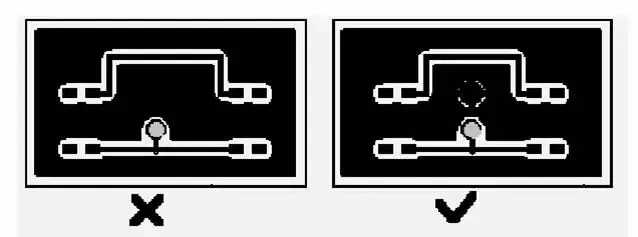
Core Principles of PCB Design
Are PCB Layout and Routing the Same for Industrial-Grade and Consumer-Grade Chips?
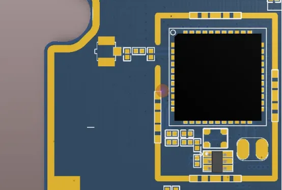
A PCB Shield Can Is Not Just a Metal Lid
Testing SW Signals in DC-DC Converters
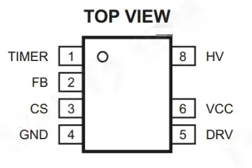
AC-DC Power Conversion: Circuit Methods, HFC0500 Example, and PCB Layout Rules
What a LISN Is and What It Is Used For

Five ESD Design Practices That Reduce Discharge Damage
VGA OUT PCB Design: Key Layout and Routing Rules
Why the Power Plane Should Be Smaller Than the Ground Plane