
pcb-integration
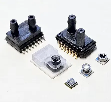
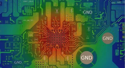
PCB integration plays a pivotal role in modern electronics design, encompassing the seamless incorporation of printed circuit boards into larger systems and assemblies. This process involves not only the physical embedding of PCBs but also ensuring optimal electrical, thermal, and mechanical compatibility with components such as sensors, processors, and power supplies. For engineers and hobbyists searching for insights on PCB integration, this tag serves as a comprehensive resource, addressing common challenges like signal integrity, heat dissipation, and space constraints in compact devices. Understanding PCB integration begins with best practices that enhance reliability and performance. Key considerations include selecting appropriate substrates, optimizing layout for minimal interference, and employing advanced techniques like multi-layer stacking or flexible PCBs for wearable tech and IoT applications. Practical applications range from automotive electronics, where integrated PCBs must withstand harsh environments, to consumer gadgets that demand efficient power management. By focusing on these elements, designers can reduce prototyping iterations, lower costs, and accelerate time to market. Articles tagged under PCB integration offer actionable guidance, from step-by-step tutorials on soldering techniques to case studies on successful system integrations in medical devices and aerospace. Whether you are troubleshooting integration issues or seeking innovative solutions for high-density designs, these resources provide expert knowledge to refine your projects. Readers interested in deepening their expertise will find the linked content below particularly valuable for exploring specific integration strategies and emerging trends in the field.
Technical Articles
Get in Touch
Send Message
- Products & Service
- Company
- About AIVON
- Contact
- News
- Blog
- Certification
-


- Payment
-


2026 AIVON.COM All Rights Reserved