The STM32F4 series implements the ARMv7-ME architecture on a 32-bit Cortex-M4F core with Harvard structure. Key features include a three-stage pipeline, Thumb-2 instruction set with DSP and SIMD extensions, single-cycle MAC, optional single-precision FPU, and configurable NVIC. The architecture supports efficient instruction fetch and data access through separate buses while maintaining a unified 4 GB address space organized in little-endian format.
AHB-Lite Bus Matrix and Master-Slave Interconnections
The main system employs a 32-bit multi-layer AHB bus matrix that interconnects eight master buses and seven slave buses. Masters include the Cortex-M4F ICode, DCode, and System buses, DMA1 and DMA2 memory buses, DMA2 peripheral bus, Ethernet DMA bus, and USB OTG HS DMA bus. Slaves encompass internal Flash (ICode and DCode interfaces), SRAM1 (112 KB), SRAM2 (16 KB), SRAM3 (64 KB on select devices), AHB1 and AHB2 peripherals, and FSMC.
After reset, peripheral clocks remain disabled except for SRAM and Flash interfaces. Each peripheral clock must be explicitly enabled via RCC registers before use. The bus bridge automatically converts 8-bit or 16-bit APB accesses into 32-bit operations.

Memory Organization and Address Mapping
Program memory, data memory, registers, and I/O ports reside within a single 4 GB little-endian address space divided into eight 512 MB regions. System SRAM (192 KB total on most devices plus 4 KB backup SRAM) supports byte, half-word, and word accesses at CPU speed with zero wait states. The 112 KB and 16 KB blocks are mapped at 0x2000 0000 and accessible by all AHB masters; the additional 64 KB block at 0x1000 0000 is CPU DCode-only on applicable variants.
Flash memory supports up to 1 MB capacity with 128-bit wide reads, byte-to-double-word programming, sector erase, and protection mechanisms. The memory is organized into sectors of 16 KB, 64 KB, and 128 KB, plus system memory and a 512-byte OTP area.
Bit-Banding for Atomic Bit Operations
Two bit-band regions allow single-bit read-modify-write operations on peripheral registers and SRAM through an alias region. The mapping formula is:
bit_word_addr = bit_band_base + (byte_offset × 32) + (bit_number × 4)
This feature is restricted to Cortex-M4F core accesses and does not extend to DMA or other masters.
Bootstrap Modes and Embedded Bootloader
Three bootstrap modes are selected via BOOT[1:0] pins sampled on the fourth rising edge of SYSCLK. Code always starts at 0x0000 0000 through the ICode bus. SRAM boot requires vector table relocation. The embedded bootloader supports reprogramming via USART1, USART3, CAN2, and USB OTG FS (DFU) interfaces, with USART operating from the internal HSI oscillator and CAN/USB requiring an external HSE clock.
Embedded System Design Considerations
High-performance AHB buses demand careful attention to signal integrity, clock distribution, and power sequencing. DMA and Ethernet/USB traffic can create bursty access patterns that stress memory controllers and interconnect bandwidth. Designers must verify that peripheral clock enabling sequences prevent bus contention and that bit-band operations remain core-exclusive when shared resources are involved.
PCB Layout and Manufacturing Implications
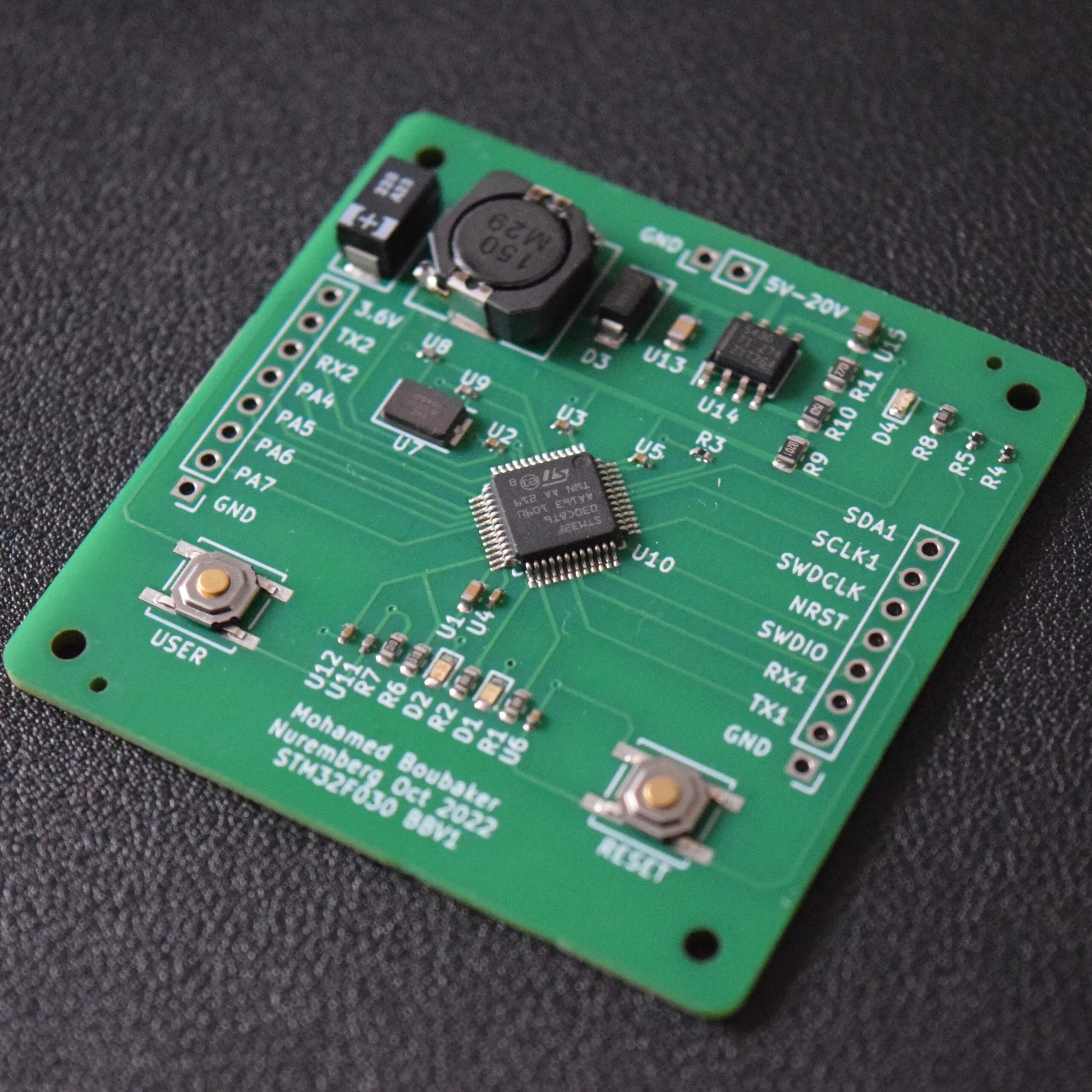
STM32F4 devices with high-speed AHB buses and multiple DMA masters require PCBs that maintain controlled impedance on address, data, and clock lines. Layer stackup design must separate sensitive analog sections from digital domains while providing low-inductance return paths. Decoupling capacitor placement near power pins, combined with appropriate copper pours and vias, minimizes voltage droop during simultaneous switching. High-density interconnect (HDI) technology supports fine-pitch BGA packages and dense routing around the MCU.
Flexible PCBs can be used for compact modules or when the MCU interfaces with moving mechanical assemblies. Material selection—low-loss laminates for RF-adjacent sections or high-Tg substrates for thermal stability—directly influences long-term reliability under vibration or temperature cycling. Thermal vias and copper balancing help dissipate heat from the core and peripherals during sustained high-load operation.
Manufacturing challenges include maintaining tight tolerances on trace widths and dielectric thickness for impedance control, ensuring via fill quality in high-layer-count boards, and performing electrical testing that verifies continuity across the complex bus matrix. Reliability engineering practices such as accelerated thermal cycling, vibration testing, and power integrity analysis are essential before volume production.
Industry Applications and Trends
STM32F4 devices appear in industrial automation, motor control, medical instrumentation, automotive subsystems, and IoT gateways. Trends toward higher integration and lower power consumption drive continued refinement of bus architectures and memory hierarchies. Electromagnetic compatibility and thermal management remain critical as clock frequencies and peripheral counts increase.
Suggested Reading: STM32 Minimal System Design Guide
Electronic Manufacturing and PCB Technologies Supporting STM32 Systems
STM32-based designs rely on multilayer PCBs with precise impedance control and mixed-signal partitioning to preserve AHB bus performance. PCB fabrication processes that deliver consistent dielectric properties and copper uniformity enable reliable high-speed operation. Assembly techniques, including precise BGA placement and underfill where required, combined with thermal management solutions, support the transition from prototype to production volumes. These manufacturing considerations directly affect system stability, electromagnetic compatibility, and field reliability in demanding industrial and automotive environments.
Conclusion
The STM32F4 memory and bus architecture provides a balanced combination of performance, flexibility, and determinism through its AHB-Lite matrix, hierarchical memory organization, and specialized features such as bit-banding. Effective utilization in embedded systems requires coordinated hardware and software design, with particular attention to bus loading, clock management, and memory protection. Printed circuit board technologies and manufacturing processes play a decisive role in realizing the architecture's full potential by ensuring signal integrity, power stability, and long-term reliability under real-world operating conditions.