










PCB Solder Mask: Essential Protective Layer in Manufacturing
PCB Solder Mask: Essential Protective Layer in Manufacturing
What This Video Covers Solder mask is far more than the green coating on a printed circuit board. This video explains its critical engineering functions in PCB fabrication and SMT assembly, showing how it controls solder flow, protects copper traces, and prevents common manufacturing defects like solder bridging and weak joints.
The presentation covers proper solder mask design rules, including pad openings, trace coverage, and via treatment (tented, plugged, or open). It highlights how manufacturing tolerances and assembly processes amplify small design decisions, and why treating solder mask DRC warnings as functional limits — not just cosmetic details — is essential for production success and long-term reliability.
Viewers will understand when to specify plugged or covered vias for higher reliability versus leaving them open for testing or secondary soldering. These insights apply directly to rigid PCB, Flexible PCB, HDI PCB, and multilayer designs used in demanding environments.
Whether optimizing a new prototype or scaling to mass production, proper solder mask implementation directly impacts yield, signal integrity, and product durability.
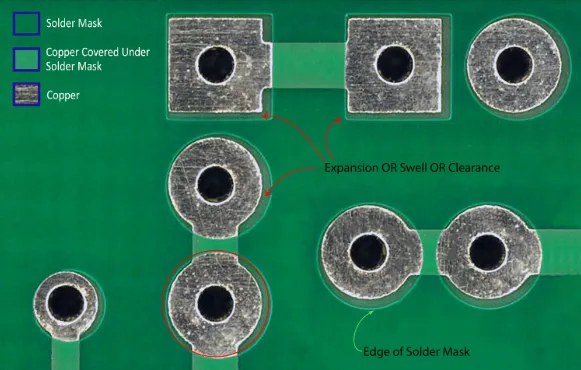
Functional Role of Solder Mask in PCB Fabrication and Assembly
The solder mask serves as a dielectric barrier applied over the copper layers of a PCB after etching. It selectively exposes component pads and certain vias while covering the majority of the copper traces. This controlled exposure prevents molten solder from flowing onto traces during reflow or wave soldering, which is a primary cause of electrical shorts and bridges in high-density SMT assemblies.
In production, solder mask thickness, color (commonly green but also available in black, white, blue, or red), and material properties (liquid photoimageable or dry film) directly influence resolution and registration accuracy. Misalignment during application can lead to exposed traces or insufficient pad coverage, resulting in solder wicking or oxidation over time. For flexible PCBs (FPC), the solder mask must also withstand repeated bending without cracking, which requires specific formulations and thickness control.
High-reliability applications such as aerospace and medical devices often demand tighter tolerances on solder mask coverage to ensure insulation resistance under environmental stress, including humidity, thermal cycling, and vibration. Production data shows that optimized solder mask designs can reduce defect rates related to solder defects by 30-50% in volume manufacturing.
Solder Mask Design Rules and Via Treatment Options
Effective solder mask design requires precise specification of pad expansions, trace-to-mask clearances, and via treatments. Standard rules include a minimum solder mask clearance (expansion) around pads of 0.05–0.1 mm depending on board complexity, while trace coverage should maintain at least 0.05 mm overlap to prevent accidental exposure.
Vias present particular challenges:
- Tented vias: Covered by solder mask on one or both sides for basic protection.
- Plugged vias: Filled with epoxy or conductive material before masking for maximum reliability and planar surfaces.
- Open vias: Left exposed for test points or additional soldering but increase risk of solder wicking and contamination.
In HDI and multilayer boards, via-in-pad designs demand even stricter control to avoid solder voids or insufficient fillet formation. Manufacturing tolerances for solder mask registration (±0.075 mm typical) must be factored into the design to avoid bridging in fine-pitch components (0.4 mm or smaller).
Common Manufacturing Challenges and Failure Modes
Poor solder mask implementation frequently leads to assembly issues. Common problems include insufficient mask clearance causing solder bridges between fine-pitch pads, excessive mask on pads resulting in poor wetting and weak joints, and via-related defects such as solder wicking that depletes solder volume on component pads.
In flexible circuits, mismatched solder mask flexibility can cause cracking at bend areas, leading to trace exposure and eventual open circuits. Environmental testing often reveals insulation resistance failures in boards with thin or poorly cured mask layers, especially under high-humidity conditions. Production EQ logs commonly reference solder mask-related DRC violations that, when ignored, manifest as yield loss during SMT or AOI inspection.
DFM Best Practices for Optimal Solder Mask Implementation
Engineers should collaborate with manufacturers early to validate solder mask parameters against specific process capabilities. Key recommendations include specifying mask color and type based on application (e.g., black for optical sensors), providing adequate clearance for high-density areas, and choosing plugged vias for boards exposed to conformal coating or harsh environments.
Always review solder mask expansion rules in the fabrication drawing and simulate assembly processes when possible. For high-reliability boards, request plugged and capped vias to create a smooth surface and prevent flux entrapment. Regular review of actual production panels helps identify registration issues before full runs.
Key Highlights
- Functional Protection: Solder mask defines exact areas where solder can flow, preventing shorts, bridging between pads, and protecting exposed copper during assembly.
- Via & Design Control: Strategic decisions on tented, plugged, or open vias, along with precise pad and trace openings, determine manufacturability and reliability under real production tolerances.
- Reliability Impact: Poor solder mask specifications lead to assembly failures; treating DRC warnings seriously sets clear production boundaries for high-reliability applications.
FAQ
Q1: What is the main purpose of solder mask on a PCB?
A1: Solder mask prevents solder from flowing to unintended areas, protecting copper traces and eliminating shorts or bridges during SMT assembly while defining precise component pad geometries.
Q2: How should vias be treated with solder mask for reliability?
A2: For higher reliability, vias should often be tented, plugged, or fully covered rather than left open. Open vias can cause solder wicking issues, while plugged vias improve durability in aerospace, automotive, and medical devices.
Q3: Why do solder mask DRC warnings matter in PCB design?
A3: Solder mask DRC warnings represent real functional and manufacturing limits, not just visual issues. Ignoring them can lead to assembly failures, reduced yield, and reliability problems amplified by production tolerances.
Q4: What solder mask clearance rules apply to fine-pitch components?
A4: For components with 0.5 mm pitch or finer, maintain solder mask expansion of 0.05–0.075 mm around pads and ensure minimum web width between mask openings to prevent bridging. Manufacturers may recommend non-solder mask defined (NSMD) pads for better reliability in high-volume production.
Q5: How does solder mask thickness affect flexible PCB performance?
A5: Thinner, more flexible solder mask formulations are required for dynamic FPC applications to prevent cracking during bending. Typical thickness ranges from 10–30 μm; excessive thickness reduces flexibility and increases risk of delamination at bend radii.
Have you ever wondered what that green layer on a PCB actually does?
Solder mask isn't just cosmetic.
It defines where solder is allowed to flow and protects copper during assembly.
By keeping solder away from unintended areas, it helps prevent shorts and reduces solder bridging between pads.
It also defines whether vias are tented or left open for testing or secondary soldering.
If solder mask design is poorly defined,issues like solder bridges, weak joints, or assembly failures can appear.
Manufacturing and assembly tolerances only amplify these problems.
Always review solder mask openings on pads, traces, and vias.
For higher reliability, consider plugging or covering vias instead of leaving them open.
Treat solder mask DRC warnings as functional limits—not visual details.
Small solder mask decisions set real production boundaries.
This is aivon,Want more PCB insights? Hit the link in bio and check out our blog!





