










Custom PCB for PS5 NAND Recycling: Turning Dead Consoles into Reliable Portable SSDs
Key Moment
- 0:00 Introduction – Previous Failed PS5 Flash Drive Attempt
- 0:30 Why Recycle PS5 NANDs (High Prices & AI Bubble)
- 1:06 PS5 Board & Flash Drive Overview
- 1:20 Compatible NAND Types (Kioxia/Toshiba Focus)
- 2:00 Flash Drive Controllers Explained (ASMedia + SM2259)
- 2:47 PCB Sponsorship
- 3:10 Removing the NAND Chips
- 3:23 Cleaning the NANDs
- 3:50 Reballing the Chips
- 6:55 Soldering NANDs to the Flash Drive
- 7:40 Introducing the MP Tool
- 9:50 Testing Controller (Removing Bad NANDs)
- 10:40 Detection Issues & Troubleshooting
- 11:00 Installing Fresh NANDs
- 11:40 Successful Detection & Configuration
- 18:00 Achieving Full Capacity
- 22:40 Assembling the Case & Final Demo
Project Background
NAND flash prices have surged under intense pressure from AI training clusters and data-center expansion. High-density packages that once sat quietly inside consumer consoles now represent scarce capacity. When a PlayStation 5 fails, its internal storage chips—Toshiba/Kioxia FBiCS4 TLC devices—are often still fully functional. Maker and engineer Chase Fournier saw an opportunity: recover those packages, place them on a purpose-built USB carrier, and create a compact, usable portable SSD that sidesteps the current supply bottleneck.

The project is more than a clever salvage exercise. It tests whether recovered high-density NAND can be reliably re-hosted on a modern controller and bridge combination, then packaged into a form factor that engineers and makers can trust with real data. Success hinges on precise PCB decisions: BGA land patterns, surface finish, via strategy under fine-pitch packages, controlled-impedance USB routing, and stable power delivery to a DRAM-less SSD controller. Without those foundations, firmware matching and capacity reporting become secondary problems that never get solved.
In this context, the carrier board is not a disposable prototype. It is the critical platform that determines whether recovered silicon becomes a daily-use drive or remains an interesting lab experiment. AIVON PCB's rapid prototyping and manufacturing support provided exactly that platform, allowing the focus to stay on electrical and firmware challenges rather than board-level defects.
What This Video Covers
The video walks through the complete workflow of recovering dual BGA132 Toshiba/Kioxia TH58LJT0T24BA4M packages from a failed PS5 motherboard and integrating them into a compact USB 3.x portable drive. It covers careful desoldering and package cleaning, reballing with a precision stencil, placement onto a custom SM2259XT + AS2235 carrier, firmware selection and programming cycles, capacity detection, performance validation with CrystalDiskMark, and real-world file-transfer behavior under thermal load. Particular attention is given to the PCB parameters that enable repeatable BGA reflow, clean high-speed signaling, and stable operation inside a metal enclosure.
Project Highlights and Key Features
- Recovered dual 512 Gb FBiCS4 TLC packages successfully reballed and mounted on a purpose-designed double-sided carrier.
- Silicon Motion SM2259XT DRAM-less controller paired with ASMedia AS2235 USB bridge for full USB 3.x compatibility.
- Detected capacity of approximately 229936 MB (~224 GB usable) after correct firmware and CE/CH mapping.
- Sequential performance reaching ~461 MB/s read and ~71 MB/s write, with practical multi-gigabyte transfers limited primarily by enclosure thermal throttling.
- Clean enumeration on PCs and multiple console USB ports, including the rear port of a working PS5.
- Controlled-impedance USB differential pairs, ENIG surface finish, filled via-in-pad under BGA regions, continuous power/ground planes, and local low-ESR decoupling—all engineered for reliability through repeated heat cycles.
- Higher-Tg FR-4 core and balanced copper distribution that maintained board flatness during reballing and assembly.
Challenges Encountered During Development
The largest technical hurdles centered on three areas. First, firmware compatibility: many SM2259XT packages refused to recognize the Toshiba FBiCS4 silicon, remaining locked in ROM mode or reporting only 1024 MB. Only a precise package–profile combination (SM2259XT2_TSB-FBiCS4_PKGW0602A_FWW0529A0 with the exact TH58LJT0T24BA4M parameters) produced a clean PASS and full capacity. Second, the AS2235 bridge required its own firmware flash and multiple plug/unplug cycles before reliable enumeration. Third, mechanical and thermal realities of fine-pitch BGA work: any solder-mask misalignment, unfilled vias that wicked paste, uneven surface finish, or board warp quickly produced opens or bridging. Sustained writes also revealed heat buildup inside the compact metal enclosure, making power integrity and plane continuity essential for stable controller behavior.
These issues are typical of high-density NAND recycling and small-form-factor USB SSD designs. Without disciplined DFM and a manufacturing partner capable of rapid, high-quality revisions, the project would have stalled at the firmware or first-pass yield stage.
How AIVON PCB Helps
AIVON PCB supplied a purpose-built custom carrier rather than a generic prototype board. The stack-up was engineered for 90 Ω controlled-impedance USB 3.x pairs, keeping the high-speed differential lines short, tightly coupled, and referenced to continuous ground planes. Surface finish was specified as ENIG, providing a flat, oxidation-resistant landing zone that allowed the reballed 132-ball packages to wet evenly on the first reflow. Via strategy under and around the BGA areas used filled via-in-pad and tightly tented microvias, eliminating solder wicking and preserving land integrity across multiple programming heat cycles.
Material selection further supported reliability: a higher-Tg FR-4 core resisted local warping during reballing, while continuous power and ground planes plus carefully placed low-ESR decoupling capacitors kept the DRAM-less SM2259XT stable under sustained write loads. Accurate soldermask registration and balanced copper distribution removed the small mechanical stresses that commonly cause opens on fine-pitch BGA assemblies.
When CE/CH mapping or resistor configurations needed adjustment for the Toshiba FBiCS4 profile, AIVON delivered quick-turn revisions of the identical stack-up and finish, keeping development momentum intact. The result was higher first-pass yield, cleaner joints, improved thermal behavior inside the enclosure, and a finished 224 GB drive that formats cleanly and survives daily use. In short, AIVON's rapid PCB prototyping, expert DFM guidance, and reliable manufacturing turned an ambitious recovery experiment into a trustworthy portable SSD.
Conclusion
Recovering high-density NAND from discarded consoles and giving it a second life as everyday storage is both technically feasible and increasingly relevant under current supply constraints. Success, however, rests on the quality of the carrier PCB: precise BGA geometry, correct surface finish, controlled impedance, robust power delivery, and the ability to iterate quickly when firmware or mapping issues appear.
AIVON PCB's combination of engineering support, fast-turn manufacturing, and attention to DFM details made that success possible. The finished drive is more than a demonstration—it is a practical, reliable product that proves recovered silicon can leave the lab and enter daily workflows.
If you are working on NAND recycling, custom USB SSD carriers, or any high-density BGA design that demands consistent reflow and high-speed signaling, start with a manufacturing partner who treats every prototype as a potential production board. Request a free DFM analysis or quote for your next carrier design at AIVON PCB and turn recovered components into working hardware you can trust.
PCB-Related FAQ
Q1: What surface finish is recommended for reballing BGA132 NAND packages onto a compact USB carrier PCB?
A1: ENIG is preferred. Its flat, oxidation-resistant surface ensures consistent wetting of reballed packages during reflow, reducing opens and bridging compared with uneven HASL finishes.
Q2: Why is via design under or near the NAND BGA critical on these carrier boards?
A2: Unfilled vias can wick solder away from the joints. Filled via-in-pad or tightly tented vias placed just outside the ball array keep solder in place and maintain joint reliability through multiple heat cycles.
Q3: What impedance control is required for a USB 3.x + SM2259XT carrier board?
A3: A controlled-impedance stack-up with 90 Ω differential pairs for the USB high-speed lines is essential. Short, tightly coupled pairs referenced to continuous ground planes prevent enumeration failures and speed loss.
Q4: How does board flatness affect yield when soldering large BGA NAND packages?
A4: Warp of only a few mils across the BGA footprint creates uneven pressure and incomplete joints. A rigid, higher-Tg board with balanced copper and proper baking significantly improves first-pass yield.
Q5: What power-delivery features are needed for a DRAM-less controller such as the SM2259XT?
A5: Place multiple low-ESR decoupling capacitors within 2–3 mm of the controller and NAND power pins, supported by continuous power and ground planes under the packages, to keep the controller stable during heavy writes.
Last year I made a YouTube video trying to turn dead PS5s into flash drives and unfortunately failed miserably. But that didn't stop you guys from watching. In fact, that video did over 200,000 views, which I am incredibly grateful for. And I'll be honest, that video has plagued me ever since I put it out.
LEAVE ME ALONE!
I have been wanting to be able to recycle these NANDs, the SSD chips on a PlayStation 5 for literally forever. Well, at least ever since it came out. But that all changes today. Today, I'm going to show you how to recycle the SSD chips on a dead PlayStation 5.
Now, I'm guessing there's probably a lot of you that want to know why were we trying to recycle NANDs? Well, the reason is because NAND prices are so astronomically high right now that if we can find different ways to recycle memory, then maybe it will actually help with the AI bubble and the price of NAND. If we can find a way to recycle NANDs that are on random devices or for instance save an SSD that has a bad controller and the NAND is still good. There's a lot of reasons. But then also, since I'm known for making flash drives, let's make one.
This is the PlayStation 5 board that we're going to be working with. And this is the flash drive we're going to be working with. I'll explain what's going on with this drive here in just a moment, but let's talk about the PlayStation 5 first.
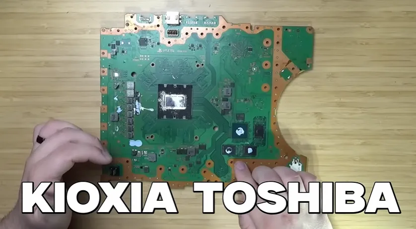
So, as far as the version of the PlayStation 5 board that you have, I don't think that matters. What matters mostly is the type of NANDs that you have. On a PlayStation 5, you can have Samsung, you can have Western Digital, you can have Kioxia Toshibas, maybe even Sandisk, but I'm not sure about the Sandisk. You can have different manufactured SSDs on your board. The ones in specific that I figured out is the Kioxia Toshiba NANDs.
So, right next to the SSD controller on the PlayStation 5, we have 1, 2, 3. Flip the board over, 4, 5, 6 SSD chips. Uh I call them SSD chips, people are going to cringe, they're NANDs. These are the chips that are very expensive right now. And it's really all because of the AI bubble. Anyways, this is all going to change right now.
So, here is our flash drive board. Currently, pay no attention to the two NANDs that are already soldered to it. These are Samsung NANDs that I pulled from a PlayStation 5 during my testing period to see if it was possible. So far, I could only get one of the chips to work, so I'm not going to be covering this in the video. I'm only going to be covering the chips that I have fully working.
The first chip we're working with is a USB controller and SATA controller by ASMedia. This chip communicates with a SATA controller and with USB and basically talks between them. This chip here is our golden child. It's the SM2259XT2G. This controller is what's going to make everything possible right now. This chip is going to interface with a NAND and allow us to talk to the USB controller and out. And yes, this controller is compatible with PlayStation 5 SSD chips.
Wait a minute. I just realized that the level of obsession that overtook me with this project, I could have just redirected that energy into creating my own custom PCB with Aivon. Aivon is a company that delivers high-quality PCBs. Now, because Aivon is so awesome, they're offering $60 for new users to go towards their PCB prototypes. That means literally, you could get your PCB for $1. So, consider trying Aivon today for your PCB project.
And now, it is time to create the PlayStation 5 flash drive. Let's do it.
First things first, add the flux. Step one, remove the IC. That's it, baby. Now, NAND number two. NAND is off.
The first step once you remove the NAND is you have to clean it. So, let's do it. Let's use the copper braid and a hot iron. Clean, clean, clean the NAND. We're going to clean the NAND because we have to get the memory recycled because the AI bubble's killing us. Yeah. Add some more flux to do and remove this human hair.
Okay, the NANDs are clean. Let's take one and then the other. We're going to put it on a paper towel with some IPA and clean them. All right, looks good enough to me. Let's reball them.
The stencil I'm going to be using is the AMAOE SSD1. And the chip we're looking at is BGA132. All right, the chip is in the general vicinity. Let's grab the stencil, put it on. Oh, there's something in that stencil. There is a bit of foreign contaminant in this stencil. Okay, that looks good. Let's try again.
Solder paste time. We just need to make sure that all this paste gets in all of the available holes so we can create balls on every single pad. That works for me. And now, let's bring in the heat.
Okay, that kind of worked. Some parts of this did not and I don't know why. Let's Okay, we're going to go ahead and do that and re-paste it again. Just like that. Try to level out the chip. You know what? I'm going to use this nice It's not a plexiglass or It's like some high temperature glass that I found on Facebook. You can buy this from like Mobile Sentrix or whatever. Anyways, you heat this up and you can pretty much watch the solder balls flow from underneath. You don't have to be as crazy and careful. It'll help from solder bridging and all that.
Okay, so if my theory is correct, with both NANDs removed, we should be able to plug this in and it should see the controller. Yep, immediately. Okay, yep, this is all correct. Now, let's plug this in. It should detect again. There we go. And we should be able to flash the firmware to it. We want to reload the firmware. We'll not do that. We'll just reload the firmware. Okay, we're going to reload the firmware. Okay, that updated. That worked. That worked. Relink worked. Perfect. And we got a pass. So, it must have been a dead NAND. I don't think it was a soldering job because I did this the other day, I had no problem. I've been doing this literally for like a couple weeks now.
So, now if we go into the MPtool, we should be able to detect the controller, the SATA controller. It should be on port one. Come on, detect it, dude. So, we either have bad NANDs or the controller died. Please don't tell me the controller died, dude. I'm going to be so sad. Oh, we see something. We see a controller. Hold up, hold up. ROM ready mode? Let's just hit start and see what happens. Oh, no, it actually worked. It actually worked, but it's going to fail because there's no flash. It is working. It's actually working. Okay, so I'm not crazy. So, we do have bad NANDs. I don't know how they're bad, but they just were.
All right, let's solder new NANDs. So, I removed the chips. We found out the controller is working. Now, uh I just installed this NAND. Now, we're going to flip it over and install the other. And hopefully, this just works. Okay, that's installed. This looks like a NAND sandwich to me. And to be honest, it looks like a delicious NAND sandwich. This is the greatest sandwich I've ever made.
We should try it and see if it works on the computer. Let's plug it in. And then we'll hit scan drive. Please find it. Please find it. Please find it. Come on. You got this MP tool. You got this. Yes, dude. Look, it's it read the flash. Toshiba. Oh my goodness. Now, it does show capacity that is 1 gig. That's because it's in ROM mode.
Okay, so let's go to parameters. Edit config. It's just the spacebar twice. Enter. And the one that we need is this one, I believe. It's either this one or this one, but I'm pretty sure it's this one. All right. Save config. And start. This is where the chili meets the cheese, my friend. If this passes MPISP and starts going okay. No, so this is not the one. All right. All right. That's okay. That's okay. That's all right.
Edit config. Okay, so then it is this other 512 gigabit one. Save. Okay. And scan the drive cuz we want to find the drive again. There it is. Yeah, and that's fine if it shows zero capacity. That's fine. It's not a big deal. All right. Download MPISP. Weird unbalanced configuration. What the heck? Hold up. Hold up. Let me double-check on this. No, that's fine. So, CE, so it does show both channels for memory. It just show our memory. So, you can see it. Why is it failing, though?
The one thing I noticed about this is that the drive shows So, the CE and then it shows the channels. So, it shows channel zero, channel one. It shows both of our memory. And then it shows also it detects that the flash is Toshiba. It checks the controller version. So, it can see everything. It can It can detect the chips and everything. So, auto says this one. I guess we can try it, but to be honest, it just failed. And my guide shows a different version. But, I don't know why my MP tool I just literally moved it cuz I did this on a different computer and then it worked. And then I just made sure to save all my things.
So, really quick, one of the variables that I changed because I just realized channel one was not selected in the previous thing. So, I went ahead. So, it's CE0. That's the CE map. And then the CH map is channel zero and channel one. Um let's save the configuration. Let's see what happens. Come on. Let's do this. It worked the other day. Why not today? I think it's working. Come on, baby. Come on. There we go. I think it's working now.
Okay, but there's a slight issue. It's not showing the whole capacity. So weird. I just dealt with this the other day with the Samsungs and I think maybe my controller there's something wrong with my controller because the other day I made a post where I actually was able to detect all of the memory, both NANDs. But now it's showing that both NANDs aren't available, which is really, really weird.
So hold up. Let's try to talk to it with the USB controller. Disconnect, reconnect. Oh yeah, see it only shows 111 gigs. That's what I'm saying. Okay. I mean, we could we could try this. I doubt it's going to work, but try to partition and format the drive. Oh yeah, there it is. That worked. Yeah, but it's only showing half the memory, which the other day it was showing all of it. Okay, so it kind of works, but it's not fully working yet. Man.
Okay, back to the drawing board. I felt that life wasn't complete if I didn't get this flash drive working. In a world where NAND flash memory is so expensive, I could only just dream of being able to recycle these NANDs. All this free memory, over 800 gigs per PS5 board, that we could just take off the board if it was only possible to have the freedom to be able to create our own drives and not have to rely on the manufacturer. We don't want crappy slow flash drives. We want our own high-quality, super fast, homemade flash drives. And not only that, but to be able to save memory that would have otherwise went to the landfill. It is now up to me to try to make this possible and the weight of that was heavy.
So this is where we're at with the flash drive. So the other day when I actually had success with this, I had just selected the NAND profile, I flashed it to the device, updated the controller's firmware, and it just worked. It showed all 230-ish gigs, 223 gigs. It's like basically it's 256, but you know how NANDs work. Anyways, what's weird is now it's only showing 64 gigs per channel, which it should be showing 120 gigs per channel. So, considering I didn't edit the NAND config profile the other day, it doesn't make any sense why this isn't working. But, I do have a hunch.
So, when I was playing around with this, because this is the the only drive that I had that had this controller on it, I I decided to try the Samsung chips on this flash drive, but the problem was it didn't work. It only showed 64 gigs per channel, just like this one. But, it doesn't make sense because why did this show and initialize all 256 gigs the other day? So, the only thing I can think of, and this is just my guess, is that maybe because I heated up the uh SSD controller so many times eventually caused an error. I don't know. There's got to be some sort of reason why it's not detecting all parts of the NAND, because these are 128 gig chips apiece, and it should be showing 223 gigs when it's fully formatted, just like it did in the screenshot. So, I'm not lying when I said I got it working. 100% I did. I showed proof that I did, but unfortunately, it's not working right now. So, my thought is we're going to have to order another flash drive and try again. See you guys in a month.
What's wrong, babe? The PS5 flash drive is a bust. And you know what? I was having issues the other day. I So, I I made the I made the I made the flash drive. The flash drive works, no problem. Then, I had to go and be the hero and try to make Samsung NANDs also compatible. And I only got them half working. Then, when I go to actually make the video, I said, "Screw it. I'm going to scrap the whole Samsung idea and just go right back to the Toshiba Kioxias." So, I put those NANDs on, and it's problem after problem after problem after problem. Nothing's working. And I checked the CE lines, and it's showing like the die on the chip is only 64 gigs in size, which is just absolutely mind-blowing cuz that's not true. Those chips are 120 gigs a piece. I don't know. I'm not sure what else to do.
I must persist forward, though. I just have this feeling in my gut that if I don't try... You know, I go by the saying, "You miss 100% of the shots you don't take." And so, I I'm trying to think. I You know, I got to know when to quit and when to keep pushing forward, and I just have this hunch where I'm like really, really close to getting this thing working again.
So, it turns out this is not 1 month later. This is actually a couple of days later. And what ended up happening was I ended up ordering another flash drive. And quite frankly, I paid a lot less than this for it. I don't know why the price went up quite considerably, but maybe this is part of the reason. I don't know. So, I just had this hunch. I decided, "What if I try to solder the NANDs again?" Because I just I I cannot let a project die until I have covered every single ground possible. So, I decided to solder the NANDs again. Then, I tried to program it, and then this happened. And then I formatted it, and then there it was.
The PS5 USB flash drive is now working, and I have it right here. This is the world's first PS5 flash drive in my hands.
Flash drive case, plastic doohickey. Let's assemble it. Now, what's kind of funny is I've never assembled a flash drive like this before. So, this is going to be interesting. Dude, I love that this is all like metallized and stuff. Come on! Come on! Come on! This is sweet. So, we have some sort of metal piece and we have this metal piece here. Wait, so how does this... Oh, that is okay. You guys are going to love this. This is so well designed. This is a nice flash drive. So, I'm going to assume that this is big USB right there and then this is USB-C and then we put the pin in to hold everything together. If the pin will go in, go in with this, right? Yeah, let's try pushing that way.
Here it is, folks, the PS5 flash drive equipped with USB-C and USB-A. Let's rock and roll with the speed test.
Okay, let's open up CrystalDiskMark. All right, yep, there's our flash drive. Hold up, let's verify. There it is, PS5 USB and I had format as FAT32. Let's reformat this. Yeah, NTFS is fine. And I guess we'll we'll go for it. All right, 3 2 1. This is USB-C, by the way. Oh crap. Holy crap, dude. Wow, that's way better than the Xbox One flash drive. Holy cow, dude. I'm stronger. I'm smarter. I'm better. I AM BETTER.
NOW, TO BE VERY CLEAR, THE WAY THIS is working is the USB controller then goes into a SATA controller that talks to the actual NANDs. Wow, man. All right, so then now it's going to do a random read, I believe, is next. And this one's going to be, I think, much lower. Okay, yeah, much lower, but definitely definitely better than the other one. Holy cow.
If you think about it, I think I spent maybe like 35-ish bucks on the flash drive. Now, they're selling for 45, which is kind of crazy. They went up $10 since I bought them. So, I don't know what's going on, but I mean, realistically, even a random read of 40 MB per second is pretty good.
All right, now it's going to do the write. We're going to see how good the write speed is on these. And I also don't know the history of these NANDs. These NANDs could be well worn out. I don't know. My assumption is they aren't because they're working really well. Okay, 71 sequential write. Okay, that's actually pretty good considering, you know, the other one sequential 461. Man, it was just warming up, baby.
Now, because this flash drive is made out of metal, it would be really cool if you put some thermal, you know, thermal conductivity inside of it. Then it would just be a a fantastic SSD. Wow, 200 MB per second random write. Amazing. All right, is this last one going to be low is my question. Quite frankly, I think this is the best flash drive I've made so far. 70. Okay, amazing. It has better write than read, which is really funny. That's uh that's incredible. All right, there we go. There's our numbers, folks.
Just for kicks, let's try to copy over a big file. I'm thinking maybe like a Linux distro. Let's just see how good it does. We got the PS5 USB and we got Ubuntu. Let's take Ubuntu and we're just going to put it on there. Oh my gosh, dude. Holy crap, dude. Okay, so they they must have Those NANDs were like, "Woah, thermal throttle." That was amazing. Wow, dude. Okay, so what we're we're we're thinking, what, maybe about a a minute a minute and a half to write the ISO is my guess. If we put some cooling on these chips, I I bet you it could it could go faster. 400 MB per second is crazy, dude. Oh my goodness. Yes, so something is getting hot is what it is. Something's getting hot, dude. Wow, I'm impressed. I'm impressed. And now it's hanging out. It's hanging out about 50 MB. Realistically, this is faster than most of the drives that I've made. So, I mean, I'll take it. This is still amazing. This is still blazing fast.
And we got Linux Mint. I can copy this one over, too. Okay, now we're increasing cuz we're near the end. All right, let's let's try to copy over Linux Mint and see how long it takes. Oh, yeah, dude, it's Shoot, man. It's big chilling, dude. It just did that whole thing. He was like, "No, dude, that was 3 gigs." That's so interesting that Ubuntu took a little bit longer and had had some issues, but Linux Mint no problem.
Okay, what about the multi-boy video that we just released not long ago? Let's copy that over, too. Okay, so now it's going a lot slower. Is it going to pick up is the question. Maybe the chips got hot, I don't know. Maybe they're they're just they're, you know, a little warm, but it's funny how Linux Mint just went boom and it was done. 3 gigs like within within 10 12 seconds not even. So, yeah, the copy test on this this drive I mean we're talking yeah, we just put 10 gigs on this drive in like 2 minutes not even like a minute. Amazing, dude.
Now, this video would not be complete without testing the flash drive on other devices. That's typically what I like to do around here. So, let's get to it.
Internal PSU modded Xbox 360 cuz why not? There we go. She booting. Plugging in the PS5 flash drive in 3 2 1. This is NTFS, so maybe I can format it. I don't know. File manager. Okay, it does not see the flash drive, but maybe that's because it's formatted in a weird way.
Okay, I just connected the flash drive to my computer. Let's format this drive to FAT32. Okay, start. Yes, close. All right. And FAT32, okay, cool. We're chilling. And we can't uh eject it, so we're just going to have to unplug it. Okay, plug it in. File manager. Dang, we still don't see it. I wonder if it detects it in the regular OS. Do we see it? Come on, Xbox. Come on, you can see it. Yes. Okay, now let's try to format it. Okay, let's configure it. It's testing the storage device. It's like I see it, but I don't know. Maybe. We're waiting patiently. It gave me the option B to cancel. Your device is ready, but it doesn't meet the Xbox 360 performance recommendations. Wow, it sees it as a 31 gig drive. It's like no, you can't have 240 gigs. You can have 32. That's all you get.
All right, now on the question is does the 32 gigs work in Aurora? Wow, yeah, there it is. Oh, now it shows it as Okay, that's hilarious. What? Wow, okay, that's really interesting. Okay, it actually shows all 223 gig odd gigs of it. That's hilarious, dude. So, it technically works on Xbox 360.
But does it work on the super hacked PS3? I don't know. Power, HDMI, okay. Are you ready? She's booting. There we go, baby. Okay, now I need some way to control it. I've literally had this controller for a millennia. All right, I'm testing the controller to see if I can get it working. I got it working, but it's a little wonky. Okay, plugging the flash drive in 3 2 1. Since my controller is wonky. Okay, flash drive just was plugged in and we see it. We see a flash drive. Now, if the controller will stop acting weird long enough to where we can go down here. No, no. We don't Oh my god. We just launched into the video creation. No, I don't want it. Information. Information is what we want. There it is. I mean, so technically it is working. It's just acting a little weird, but that's fine. Now, the reason it's showing 191 gigs is because the way we formatted it with the Xbox 360, but we're going to stick with that format for now just because for some reason GUI format with the FAT32 situation didn't really work, but that is totally fine. We're seeing 191 gigs on this PS3 and it's actually working.
9.0 jailbroken PS4 time. Does the PS5 flash drive work on a jailbroken PS4? Power, HDMI. Let's turn it on, baby. Or maybe not. Is it plugged all the way in? Did my PS4 die? Okay, that that yeah. Oh, now it works. All right, HDMI, plugging it in. And why not plug in the flash drive? Okay, flash drive's plugged in. There we go. All right, web browser. Jailbreak the console, please. Okay, I'm just going to let it sit for a second. Oh, yep, it ran. Beautiful. All right, we're now jailbroken. Now, let's test the flash drive. And down in the corner we see mount USB 0 223 gigs. It detects the whole thing, dude. Let's go. That's amazing. Now, I'm also curious if it detects it in settings like storage settings. I wonder if it sees it. USB storage devices. Yeah, and it sees it. Here it is. Can we actually format it as extended storage? Yes, we could. And it sees that the format option is fast. So, it's actually working. That's amazing.
Now, does this flash drive work on the PS5? Let's find out. Okay, the time has come. Does the PS5 flash drive work on a PS5? Let's plug it in USB-C cuz why not? Settings, storage, USB extended storage, devices maybe, system. I actually don't know how to check. Storage, console storage. Maybe the USB-C doesn't work on the front. Maybe USB-C doesn't work on my PS5. Okay, let's try big USB cuz I'm pretty sure that that works. Big USB, wow. Is this really where it ends? Not like this. Not like this. Accessories, do we see it in here? System, backup. Let's see backup to. There's no USB drive connected. Does it not detect it on the PS5?
All right, let's try the back USB port. Okay, connected the flash drive to the back USB port. Now does it work? Okay, system, backup. Let me just see if it Wait, it sees a flash drive. Apparently my front USB ports don't work. Hold up, hold up, hold up. Storage, USB extension. There it is, baby. Yes, it shows. It shows. So apparently my front USB ports don't work and only the rear ones do. So I'm going to look into that. But there you go, folks. The PS5 flash drive works on a PS5.
Now that we know that the PS5 flash drive is now possible, where should I try the flash drive next? And by the way, YouTube thinks you should check out this video right over here.





