










AIVON PCB Enables Reliable BadWDSD PS3 Firmware Time Travel
Key Moment
- 0:00 Introduction – Modded PS3 Won’t Boot
- 0:26 Diagnosing Disconnected Modchip Wires
- 1:00 Resoldering with Thicker Enameled Wire
- 2:00 Rerouting & Securing the Wires
- 2:50 Applying Solder Mask & UV Curing
- 3:07 AIVON PCB Sponsorship
- 3:40 Preparing for Test Boot (Outside Case)
- 4:30 First Boot Attempt & Flasher Mode
- 5:00 Trying Recovery Mode Buttons
- 5:50 Reflashing NOR (Corrupt Backup Fixed)
- 6:20 Successful Boot Demonstration
- 7:00 Showing Stock 4.82 Firmware
- 8:00 Entering Downgrade Mode (Firmware 3.66)
Project Background
In the competitive world of console homebrew and hardware modification, late-model PlayStation 3 units—particularly the CECH-3000 series—have long been considered locked and resistant to custom firmware. Official hardware restrictions prevent straightforward firmware downgrades, limiting enthusiasts and developers who need access to older system versions for quasi-CFW, Cobra features, or specialized diagnostics. Chase Fournier set out to change that reality with an ambitious goal: transform a "bricked" or unstable retail 3000 into a true firmware time machine capable of safely moving between versions that the board was never designed to support.
The project demanded far more than software. It required precise understanding of high-speed signal integrity across a real motherboard, mechanical reliability under vibration and thermal cycling inside a closed chassis, and manufacturing discipline that turns a one-off bench success into something other makers can repeat. The core tool was a Raspberry Pi Pico running the BadWDSD exploit, carefully interfaced to the XDR RAM and Syscon lines. Success hinged on the physical connections—especially the critical CMD and CLK nets—remaining short, low-inductance, and mechanically locked. This is the environment where professional PCB manufacturing and rapid prototyping become decisive.
What This Video Covers
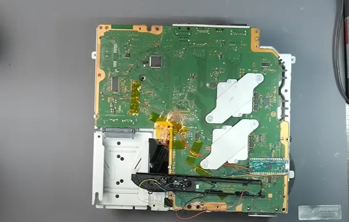
The video opens with a CECH-3000 that powers on, beeps, and immediately shuts down—classic symptoms of failed XDR initialization caused by compromised CMD and CLK connections. Chase diagnoses two wires that had worked themselves loose under normal handling and vibration. He replaces them with properly gauged enameled magnet wire, cleans the insulation, applies fresh flux, and re-solders under magnification. A thin layer of UV-curable solder mask locks the runs in place. After an isopropyl clean and a corrected NOR flash, the console stabilizes on stock 4.82 firmware.
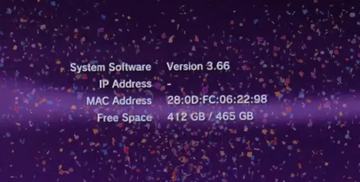
With hardware integrity restored, the demonstration shifts to the project's defining capability: loading and accepting a 3.66 firmware image that should have been impossible on this board. The install completes, the system reboots, and the classic PlayStation logo appears on the older firmware—the first documented successful retail 3000 firmware time travel. The same modchip then enables full qCFW based on Evilnat PEX, supporting most Cobra features while still allowing a safe return to official firmware via the BANKSEL pin or a standard PUP reinstall. Optional DEBUG UART access at 576000 baud provides direct Syscon visibility for deeper diagnostics.
Throughout the process, the video repeatedly returns to the physical realities that determine long-term success: wire length and gauge, resistance verification, power and ground distribution, surface finish quality, and mechanical retention. These are not secondary details; they are the difference between a working prototype and a reliable, repeatable modification.
Project Highlights and Key Features
- First documented retail CECH-3000 successfully downgraded from 4.82 to 3.66 firmware while remaining fully functional.
- Raspberry Pi Pico-based BadWDSD implementation delivering precise code injection into XDR RAM at the required timing window.
- Short, low-inductance CMD and CLK runs (target ≤ 80 mm) using 0.1 mm magnet wire to preserve high-speed signal integrity.
- Verified post-solder resistance of approximately 55 Ω to ground as a practical reality check for connection quality.
- UV-curable solder mask providing simple, effective mechanical strain relief that prevents wire migration under vibration.
- Full qCFW support with Evilnat PEX, most Cobra features, and reversible return to official firmware.
- Optional high-speed DEBUG UART (576000 baud) for real-time Syscon monitoring.
- Emphasis on clean power and ground distribution using heavier conductors than signal nets.
- Practical demonstration of recovery from both mechanical (loose wires) and data (corrupt NOR) failure modes.
- Clear DFM principles that scale from a single Pico installation to custom RP2040 carrier boards.
Challenges Encountered During Development
Even after an initially successful install, real-world conditions quickly exposed vulnerabilities. The original signal wires loosened under vibration and thermal cycling inside the console chassis, collapsing the boot chain and producing continuous power cycles. Excess length or incorrect gauge on the CMD and CLK nets introduced enough inductance and resistance to prevent proper XDR RAM initialization—manifesting as the stubborn "green light of death" or repeated shutdowns.
A second critical failure appeared when the NOR backup itself proved corrupt. The console reached a partial boot state and stalled, turning a recoverable situation into a near-brick until a verified, checksum-checked image and an E3-style flasher restored functionality. Flux residue left after rework and unsupported wire runs remained persistent long-term reliability risks. These issues are classic illustrations of incomplete design-for-manufacturing thinking: signal paths and power paths must be treated as distinct problems, mechanical retention must be designed for the actual operating environment, and every critical flash image must be verified before trust is placed in it.
When builders move beyond a bare commercial Pico to custom carriers or breakout boards, the same challenges multiply. Insufficient clearance around fine pads, unbalanced copper, inadequate via technology, or the wrong surface finish can destroy first-article yield and force repeated rework. Timeline pressure in the modding community leaves little room for iterative board failures; each unsuccessful prototype costs both money and momentum.
How AIVON PCB Helps
Chase's working console proved the exploit and the software stack. Scaling that success so other makers can replicate, improve, and trust the result requires boards that arrive with consistent electrical and mechanical quality. This is precisely where AIVON PCB's rapid prototyping and precision manufacturing become the enabling foundation.
When designers create cleaner RP2040 carriers, better strain-relieved pads, Syscon breakout boards, or experimental interface boards that keep CMD and CLK runs short and well-referenced, they need prototypes that measure correctly the first time. AIVON's quick-turn service delivers controlled stack-ups and higher-Tg FR-4 materials (Tg ≥ 150 °C) that provide the thermal stability required inside a closed console experiencing repeated power cycles. Consistent 1 oz copper weight and ENIG surface finish produce flat, oxidation-resistant pads that accept fine magnet-wire soldering cleanly and survive multiple rework sessions without lifting or degrading.
Proper via technology and tight manufacturing tolerances keep impedance and inductance low on the critical high-speed nets, directly supporting the narrow timing window the BadWDSD exploit depends on. Responsive DFM feedback catches issues—insufficient clearance around fine pads, unbalanced copper distribution, or missing mechanical retention features—before the boards ever leave the factory. The result is a carrier or breakout that simplifies assembly, dramatically reduces intermittent connections, and raises the overall success rate from "it worked once on my bench" to "other people can build this too."
In practical terms, AIVON's boards improve voltage stability during the sensitive XDR injection window through cleaner power and ground distribution. Reliable plating and consistent solderability let makers lock wires with solder mask more confidently, addressing the exact mechanical failure Chase had to correct by hand. Fewer first-article surprises mean the builder can focus on firmware behavior and recovery paths instead of chasing board-level defects. Whether the need is a simple 2-layer carrier for short signal runs or a 4-layer design requiring tighter impedance control and denser routing, AIVON's one-stop rapid PCB manufacturing, expert DFM analysis, and reliable delivery turn experimental concepts into production-ready hardware.
Conclusion
Chase took a console that refused to stay powered on and turned it into the first retail 3000 capable of genuine firmware time travel. The path ran through careful soldering, short signal runs, verified flash images, and mechanical retention that survives real handling. The same principles scale directly to any custom board a maker designs around the BadWDSD exploit or similar high-speed injection techniques.
Clean layout practices matter. Manufacturing partners who treat every prototype as if it has to work the first time matter even more. If you are developing a custom RP2040 carrier, a high-speed signal interface board, or any precision modchip solution that demands reliable fine-pitch soldering, controlled impedance, and mechanical durability, start with a partner who delivers consistent quality and expert DFM support.
FAQ
Q1: Why does CMD/CLK wire length and gauge matter so much for BadWDSD-style PCB installs?
A1: These nets carry the high-speed XDR interface used by the exploit. Extra length or incorrect gauge adds inductance and resistance that can prevent proper RAM initialization. Keep runs under 80 mm with 0.1 mm magnet wire and verify roughly 55 Ω to ground after soldering for reliable operation.
Q2: What surface finish is best for fine hand-soldering on a custom RP2040 BadWDSD carrier PCB?
A2: ENIG is preferred because it provides a flat, oxidation-resistant surface that accepts fine solder joints cleanly and survives multiple rework cycles without degrading pad quality—critical for magnet-wire connections and long-term reliability.
Q3: Should I choose a 2-layer or 4-layer PCB for a custom BadWDSD carrier board?
A3: A well-laid-out 2-layer board is usually sufficient for short signal runs and basic power distribution. Move to 4-layer when tighter impedance control, better ground planes, or denser routing around the Pico and connector areas is required.
Q4: How does solder mask improve long-term reliability of modchip PCB assemblies?
A4: A thin, properly cured solder-mask layer locks fine magnet wires in place, prevents migration under vibration, and reduces the chance of accidental shorts. It is one of the simplest and most effective mechanical retention methods for boards that live inside closed consoles.
Q5: What DFM checks catch the most common failures before ordering a prototype from AIVON PCB?
A5: Confirm short critical-signal lengths, adequate copper for power and ground, proper pad sizes for hand soldering, and sufficient clearance around high-speed nets. Requesting manufacturer DFM feedback on these points prevents most first-article problems and improves yield.
PS3 time. Huh? So, yeah. This is my hacked PS3. This is the one that is running the bad WDSD modded chip. All right, so here's the deal. Console doesn't boot. Turns on, shuts off. I think it's something to do with the mod chip and the wires that have come disconnected. So, let's fix it.
So, according to this diagram, I had these wires soldered up here. I was honestly afraid of breaking them at points on these components here. So, I soldered them up here. This one's still connected and this one... Where did this even... Where did I even solder this to? I honestly don't remember, but it was somewhere anyways. So, these wires need to be unrun and then rerun. I guess we'll start with this one.
All right, so this is one of them. Let's disconnect this wire here. Boom. Let's add a little bit of flux to that point there. And I'm actually going to use some of this thicker wire that's enameled instead. Hopefully, this will serve as a better connection. To be honest, I'm not 100% sure, but it probably will be.
All right, so I'm going to kind of like loosely run the wire over here and then I'll tuck it under some things and then like solder mask it in place. Okay, so let's just cut the wire here like that.
As for the other wire, um dude, I am so sorry for my wiring job. It is atrocious. Oh. Absolutely atrocious, but that's fine. Let's uh come on over here. We'll disconnect this wire from this point here. Come on. There we go. All right, then we'll go back over here. Add a little bit of flux, add some solder. All right, solder our wire. And we're also going to cut this wire right there. That's fine.
All right, now let's run the wires. So, the first one will go under here like that. Right over to this point here right here. So, let's grab the micro pencil micro soldering iron. Solder there. We'll also add some solder to the end of this, burn the enamel on this wire, and then we'll connect the wire. Connect the wire in 3 2... Why am I having trouble? There we go. And then we'll run the second wire. Okay, let's burn the enamel off of this one, and then just like that. That's it. Should be good.
Let's grab a little bit of isopropyl alcohol and a brush, and then grab the old blower and try to clean the board. Blow it away. All right, perfect. That works. All right, let's do that. We'll just add a teensy weensy bit of solder mask to this area. Perfect. Yeah, I would think I would prefer to always add solder mask after you run these wires just because like you don't want them to move from that location. You want them to stay, and that was my problem. They kept falling off. Maybe I was just using wire that was too thick.
All right, let's grab the UV curing light. Oh guys, don't look at this. Just kidding. Grab the UV curing light, you know, the black light, and we'll cure this just like that. All right, perfect. All right, fam. We went ahead and cured this mask.
Okay, so what now? Well, I guess we can we can test the console. We can see if it works.
Have you ever thought about making a PS3 yourself? Well, do I have the solution for you? This video is sponsored by AIVON. AIVON is a company that delivers high-quality PCBs. So, if you wanted to design your own PS3 PCB motherboard, you can technically do it through KiCad and then send it to AIVON, and then they'll make it for you. Now, because AIVON is so awesome, they're offering $60 for new users to go towards their PCB prototypes. That means literally you could get your PCB for $1. So, consider trying AIVON today for your PCB project.
Let's plug in this hard drive. There we go. Very carefully lift this up like that. Yeah, cuz we can test this outside of the case, I think, without any problems, potentially. Let's grab a piece of paper towel just to insulate the E3 flasher like I was doing with the power supply, the top case that has the E3 flasher attached to it. And then we need the plug to power cord. Let's plug in the power supply. All right, plug in the power cord. 5-volt 5-volt standby, okay. Plugged in.
All right, now we need to move this out of the way. Grab our flasher cable very very very carefully. Grab our flasher and this very very carefully plug in this to the flasher. Very carefully. Don't drop that. All right, beautiful. Okay.
All right, now guys, we should be able to see if the PS3 makes a triple beep when we turn this on. I believe the mod chip worked. Plug this in. All right, wait for this to go solid. All right, and then turn it on. All right, hard drive activity. Oh, it's got my bad. This is This flasher is set to be in fun flash mode, which means it halts the PS3 boot time. Turn that switch off. Now this will be a legit test, okay. Hard drive should read. Beep beep beep beep beep. Is this going to stay on? Guys, I think we did it. We just have to wait and see if we get hard drive activity. We get hard drive activity. Dude, if it was just the two wires and this whole thing works again, that'd be insane.
Console shut down. Uh shoot, what do we try next? Do we try the recovery mode? I don't remember which button I made the recovery mode one. It's either this one or that one. Uh well, I don't know. I guess the only way to try is to plug in the console and hold one of the buttons down. I'm going to guess it's this one. That's not it, all right. Let's try this one. Nope, cuz it didn't auto start. Let's try this one. Yep, that's the recovery mode button. Okay. Now if we continue to hold it, actually I think we're good. 3 4 5 6 7
I think it's fixed, but I'm not 100% sure. So, this red light here is actually the light from the Pico on the bottom of the console. So, the console is getting to a part where it seems like it's working but...
We reflash the NOR chip by flipping the flasher switch and starting the process, waiting for 100% progress. The NOR flash backup was corrupt, so it is fixed, reloaded onto the SD card, and reflashed, restoring functionality.
With the console working, the Pico's LED must stop blinking before powering on, waiting for a triple beep indicating the mod chip's success. Hard drive activity confirms booting, and the console displays on a monitor as a stock 4.82 model.
Downgrading begins by unplugging power, plugging in a USB with 3.66 firmware, and holding a button to enter downgrade mode, which auto-starts the console.
After booting into recovery mode (confirmed by a beep), a controller is connected. The console accepts 3.66 firmware from 4.82, despite attempts to go lower (like 3.60 or 3.55) failing. The installation completes with flashing hard drive activity, leading to a reboot. Initial boot issues arise, requiring multiple reinstalls of the firmware to match ROS versions (0 and 1).
Further troubleshooting involves unplugging and replugging power quickly to disable the mod chip before initialization, achieving a successful boot to the PlayStation logo on 3.66.
The console is now a retail unit on 3.66, credited to Kufu and the PS3 hacking team.
Thanks for watching.





