










Polaroid Digital Frame PCB Reverse Engineering: Building a Custom SPI Flash Adapter
Key Moment
- 0:00 Introduction – Buying the Polaroid Frame
- 0:40 Unboxing & First Look
- 1:30 Power Specs & Initial Thoughts
- 2:02 AIVON PCB Sponsorship
- 2:30 Powering On the Frame
- 3:00 Starting Disassembly
- 4:00 Removing the Screen
- 5:00 Board Inspection Under Microscope
- 6:00 Identifying CPU & Components (MIPS)
- 7:00 Planning to Dump the ROM
- 7:40 Removing the BIOS / Flash Chip
- 9:30 Chip Removed & Next Steps
Project Background
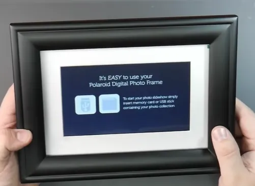
There is a special kind of satisfaction that comes from rescuing a forgotten piece of consumer electronics and turning it into a serious learning platform. In this project, hardware enthusiast Chase Fournier picked up a Polaroid 7-inch high-resolution digital picture frame at Goodwill for roughly fifteen dollars on half-off day. The unit featured a wood-look frame, mat, near-720p screen, SD and USB inputs—the classic early-2010s digital photo frame that once sat on countless shelves cycling family pictures.
Chase already had a Sony frame project on temporary pause because its CPU architecture felt unfamiliar. This Polaroid looked like a better entry point. His goal was straightforward and honest: open the device, map the hardware, dump the firmware, and eventually understand the board well enough to talk to it. There were no flashy ambitions of running Doom on a photo frame—just pure curiosity and the desire to reverse-engineer a real commercial PCB.
That kind of curiosity lives or dies on solid PCB work. The original board is a compact L-shaped multilayer design with tight component placement, an empty NAND footprint that hints at design evolution, and a 4 MB SPI flash that holds the keys. Getting clean, repeatable access to that flash without destroying the only sample is pure DFM reality: pad integrity, thermal control, and reliable interfacing. This is exactly where professional PCB manufacturing and rapid prototyping capabilities become essential partners rather than afterthoughts.
What This Video Covers
This video walks through the complete reverse-engineering journey of the Polaroid digital picture frame, from initial power-on and teardown to successful SPI flash extraction and the creation of a purpose-built debug adapter. Viewers will see the careful disassembly process, identification of key landmarks on the L-shaped motherboard (MIPS-based multimedia processor, 3.3 V regulator, USB and SD/MMC connectors, empty NAND pad, and the critical 4 MB SPI flash), the chip-off procedure, firmware dump, and the transition from a fragile homemade adapter to a professional custom PCB. The content also covers real bench challenges, DFM considerations for chip-off and interposer boards, and how a fast-turn, high-quality prototype board transformed a one-time lucky dump into a repeatable hardware platform.
Project Highlights and Key Features
- Compact L-shaped multilayer PCB designed to fit inside a thin digital frame housing, featuring classic cost-optimized consumer electronics choices.
- MIPS multimedia SoC (exact variant still under identification in episode 1) paired with a 4 MB SPI flash in SOIC-8 package and an unused NAND footprint that reveals design evolution.
- External DC jack feeding a 3.3 V regulator with no USB power path, plus interfaces for USB, SD/MMC, screen ribbon, button flex, and IR control lines.
- Successful non-destructive (to the original pads) chip-off of the SPI flash, followed by a clean 4 MB dump containing readable strings such as storage.bin, welcome.bin, FB.BIN, startup test LCD.bin, "enter debug mode," display enable, speaker on, and hard-key shut-off.
- Firmware that is not encrypted and shows a recognizable file-system structure, immediately opening the project to further exploration.
- Purpose-designed SPI flash breakout and debug interface board manufactured by AIVON PCB with perfect SOIC-8 footprint, generous annular rings, on-board decoupling (100 nF + 10 µF), level-shifted SPI, selectable 3.3 V / 1.8 V operation, labeled test points, and a 2.54 mm header bringing out CLK, MOSI, MISO, CS, and a dedicated UART pair.
- 1.0 mm FR-4 with ENIG finish for mechanical strength and repeated rework capability under microscope or programmer clips.
- Full DFM review prior to fabrication that caught a keep-out violation near the SOIC pads and a slightly undersized via, resulting in precise soldermask registration, clean edge plating, and consistent impedance on short SPI traces.
Challenges Encountered During Development
Nothing about reverse-engineering a sealed consumer board is trivial. The first major hurdle was cleanly removing the SPI flash. Reflow with flux, careful lifting with tweezers and an X-Acto knife—any slip risks lifting pads or destroying the only available chip. Once free, the next problem appeared immediately: the pads on the initial programmer adapter board were simply too small. Soldering the fine-pitch flash legs became a real struggle; alignment was difficult and the iron would not wet the joints reliably.
Chase's temporary solution was pure maker ingenuity—he stacked the undersized adapter onto a larger carrier board to gain mechanical stability and finally achieve solid electrical contact. It worked for one successful dump, but it was a classic "this should not have been this hard" moment. The same session also required a quick repair to a previously voltage-modded pin on the programmer that had been damaged earlier.
Additional ongoing challenges included locating an unmarked UART on the dense L-shaped board, keeping the fragile screen connector and flex cable intact, and mapping the exact MIPS multimedia processor variant once readable strings began appearing. These are the exact pain points that turn a fun Saturday project into a multi-week saga. They also highlight why DFM thinking matters even on the reverse-engineering side: good annular rings, solid pad design, accessible test points, and proper surface finish make later analysis far less painful and far more repeatable.
How AIVON PCB Helps
This is where the story changes from clever soldering to professional capability. Chase needed a clean, repeatable way to interface with the 4 MB SPI flash without gambling the original pads every single time. The homemade stacked adapter was good enough for one dump, but it was not something that could be relied upon for the next ten experiments, for writing modified firmware, or for bringing UART and power monitoring out to proper headers.
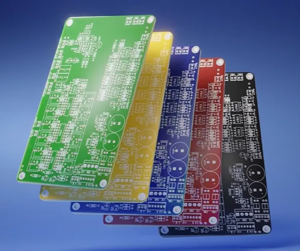
AIVON PCB produced a small, purpose-designed SPI flash breakout and debug interface board engineered specifically for this style of work. The design goals were simple but non-negotiable: perfect SOIC-8 footprint with generous annular rings so the flash can be soldered and desoldered multiple times without pad failure; on-board 100 nF + 10 µF decoupling right at the power pins so the programmer sees a clean rail; level-shifted SPI and optional 3.3 V / 1.8 V selection so the same board works with different programmers; clearly labeled test points and a 2.54 mm header that brings out all critical signals plus a dedicated UART pair; and mechanical strength via 1.0 mm FR-4 with ENIG finish so the board can sit under a microscope or be clipped into a programmer day after day.
AIVON's engineering team ran a full DFM analysis before the panels were cut. They caught a keep-out violation near the SOIC pads and a slightly undersized via that would have caused yield loss. The boards returned with precise soldermask registration, clean edge plating, and consistent impedance on the short SPI traces.
The difference was immediate. Chase could now remove the original flash once, drop it onto a reliable carrier, and work for hours without intermittent contact or damaged pads. The same board later became the foundation for permanent debug wiring that will stay with the Polaroid frame through future episodes. Manufacturing precision mattered. Fast turnaround mattered even more. When a reverse-engineering session is hot, waiting two weeks for boards kills momentum. Receiving five perfect adapters in a few days kept the project alive and moving forward.
In short, the original Polaroid board gave Chase the firmware. The AIVON custom PCB—produced with rapid PCB manufacturing, expert DFM analysis, and high-reliability finishes—gave him a professional, repeatable, and safe way to keep exploring it. That is how a $15 Goodwill find turns into a real hardware platform instead of a one-time lucky dump.
Conclusion
Chase ended episode 1 with a successful 4 MB dump and a list of readable strings that already point toward debug modes and file-system structure. The Polaroid is still in pieces, the MIPS core is still being researched, and UART has not yet been located—but the foundation is solid.
That is the real joy of these projects. A cheap consumer board, careful hands, and the ability to spin reliable supporting PCBs when needed turn "I wonder what's inside" into actual progress. If you have a similar frame sitting in a drawer or a new idea that needs a quick adapter board, the path is clearer than it looks. Document everything, respect the original pads, and when you need a clean prototype, treat manufacturing as a partner rather than an afterthought.
PCB-Related FAQ
Q1: What is the safest way to dump an SPI flash from a consumer photo-frame PCB?
A1: Prefer a test clip if the package allows it. When desoldering is required, use plenty of flux, controlled hot-air, and a good preheater. Always verify the chip’s voltage and pinout against the datasheet before powering the programmer. If mounting the chip on a new adapter, double-check pad size and annular ring first.
Q2: Why do so many low-cost digital frames use SPI flash and relatively simple board constructions?
A2: Cost and simplicity. A small SPI NOR keeps the BOM under control while still providing enough storage for firmware and assets. Multilayer or more complex memory appears only when Wi-Fi, higher resolution, or additional power domains are required.
Q3: How should I design a reliable breakout or interposer for repeated SPI flash work?
A3: Keep the original footprint geometry exact, make the pads generously long, add test points on every SPI line, use a standard 2.54 mm header for the programmer side, include proper decoupling, and always request a free DFM review. ENIG finish and 0.8–1.0 mm board thickness improve rework durability.
Q4: Is it worth ordering professional PCBs just for a reverse-engineering fixture or chip-off adapter?
A4: Absolutely. A clean, labeled adapter with properly sized pads and test points saves hours of probing frustration and dramatically reduces the risk of damaging the original device. With rapid PCB manufacturing and competitive prototype pricing, the barrier is low and the reliability gain is high.
Q5: What key DFM items should I double-check before sending Gerbers for a photo-frame-style mod or adapter board?
A5: Minimum annular ring and pad length for the flash footprint, solder-mask dams between fine pads, via treatment, outline-to-copper clearance, and any mechanical features that must match the original housing. A thorough DFM review will flag undersized pads or keep-out violations before fabrication starts.
Okay, I must admit something. I bought another one.
So, if you don't know, I was trying to hack the Sony photo frame, and I still am, but it is on a brief hiatus for now.
In the meantime, I picked up a Polaroid 7in high-res digital picture frame, and it has wood art and a mat allegedly.
Yes, I paid 29. No, I did not. I paid half. It was half off day at Goodwill. So that means I paid about $15 for this thing.
And in this video, we're going to open this up and see exactly what is going inside this photo frame. And then we are going to allegedly attempt potentially hack this thing.
All right, let's try to get in there. Get in there, sir. There we go.
All right, we're in, fam. Inside the box, we got we got a manual. Hopefully it tells us what CPU type it's got.
Here it is. Oh my god, look at that bezel. Dude, this is actually This is really nice. I'm going to be kind of sad to hack this thing, NOT GOING TO LIE.
ALL RIGHT. What do we got? We have a stand that screws onto the back, which we're not going to use for now. And we have the quick start guide.
It It says, “Attach the stand, plug it in, power it on, insert a memory card, and things like that.” And then we also have it in I think that's Spanish.
You know, I don't speak Spanish.
Okay. So, photoframe. What does this take? Uh DCN. It says DCN, but it doesn't tell us how many DC volts it takes. This is This is a 5V. Is this USB? No, this is not USB. just a just a DC jack.
Well, shoot. Let's plug it in and see what it does.
Now, I'll be honest for a moment while we're trying to get this power cord undone. My problem with the Sony photoframe project is the CPU architecture. I am not familiar enough with the CPU architecture to create uh a exploit. I'm really I'm not qualified to do that in the first place.
But I figure if we can find a device that has some known things that maybe we could try to sort of learn and hijack the software to, you know, end up doing things. And so that's why I was like, well, let's try to hack a Polaroid.
Wait, wait, wait. This video is sponsored by Iwan. Ian is a PCB manufacturing company that supplies highquality PCBs directly to you.
So, let's say you just designed a PCB and you really, really just want to have it made and on your desk so you can start soldering components or you want to just have them do it for you. Iwan offers that.
They're currently offering $60 towards a new user. So that means you can get your PCB prototype for literally $1. Consider trying Iwan for your next PCB project.
Okay, DC power. Plug it in. Is there a power button? Oh, yep. There is. It's turning on. It's turning on.
So, this is the top. Ooh, there's still a screen protector thing on it. Oh, and it's an almost 720p. Ooh, interesting.
To start your photo slide, simply insert memory card or USB stick. Very interesting.
Okay. Um, I think that's all we need to know about this.
Oh, you know what's really, really funny? I'm just now noticing this. Dude, this is just like a regular picture frame. It's got a screw here, here, here, and here.
So, this means this should come apart pretty easily, right? Right.
All right, let's take Oh, we might We might not even have to take the screw all the way out. Are you serious, bro? Come on. No way it's like that.
Well, shoot. Dude, let's just do that. That does this just come out. Dude, this is way better than the Sony frame. Well, only part is is it's probably cheaper. Okay, never mind. It's not better than the Sony frame. I hate this. I absolutely hate this.
Okay, cuz then we're going to get fingerprint smudges all over the screen. Then this is what we're going to do. Let's take out these screws. I see here. One, two, three, and four.
And then, oh, okay. Okay. And then just the screen comes out. Okay, that is that is bizarre. Okay, interesting.
I'll set the screen off to the side. I guess I'll put these back on since technically it can just come out with those four screws. This is weird, dude. I don't know if I like this now. It's making me feel confused. It's like a traditional picture.
What's funny is you could actually just take this and literally put your own picture in this.
I see the ribbon cable. Oh, wow. This is way smaller than I was expecting. Oh, here we go. All right, let's disconnect the screen. Screen is disconnected.
I'm presuming this is probably the CPU. Uh, what else do we have here? We have USB. We have This is SD. We have power. We have SD and MMC. Here we have the power jack. We have USB.
What else do we got? Oh, we have a 3.3 voltage regulator. We have a power cable that goes to a board here. This is for the buttons.
Okay. Do we have anything on the underside of this board? I'm going to take out this one screw right here. Oh, no. There's two screws. I think I see two. One screw out. And there's the other one. Let's take out this screw.
Now, the board should just come out like nothing. And we can unplug this. There we go. And take a look at the other.
I see something. Dude, there was a NAND that sat here at one point. It was designed this way.
Okay, this is the border vision. This is what it looks like. 2019. Ooh, 2030. Okay, this is definitely an SBI flash. And I bet you ooh IRVCC ground and IR. So that must be what would have been if this was a better model would have had a remote.
That is intriguing. Okay. Okay. Okay. So, since the board is in the shape of an L, the only thing we have over here is the screen. the connector for the screen. We do have an IR ground and IR VCC, so power, I'm guessing.
Um, we have a BIOS, like a flash ROM here. Um, the CPU is definitely this guy. And this CPU, I have to figure out exactly what it is. I'll have to do a little bit of research, but I bet that if we can figure out what this is, and we figure out what this is, then if we can figure out the architecture, when we dump this, we should be able to have a look at the ROM. and then we should be able to program something potentially if the CPU architecture is good enough where we can have something available.
Um the other thing is unless we can figure out where UART would be on this board. This board is tiny so it's kind of tough to say. Maybe maybe UART's over here. Maybe I'm trying to think of where UART could be at. I mean could this be UART? No, I doubt it. But maybe like probably not.
All right, let me look up the CPU and see what I can come up with.
Okay, fam. I did the research or at least most of the research. I I believe this is a MIP's processor. Apparently, from what I am seeing, this is a multimedia uh processor. Obviously, considering that it's in a photo frame, that's probably what it is, right?
So, here's the deal. I don't know where UART is on the board yet. That is something that we will discover. The other thing is, since I don't want this video to be super short, we're going to attempt to dump this ROM right now. Like, no. Like, seriously. Right now, I've got the I've got the CH programmer right here. Let's Let's do it.
I just realized something. This was voltage modded until it wasn't. So, the pin's kind of messed up. Now, we have to fix this.
All right, it's fixed. We got it. Now, we need to remove this BOS chip. So, I think that best and easy way to do this is going to be to reflow all of these connections, these connections just like that. Then come around this way. Refflow these. And then we should be able to grab a pair of tweezers.
We're going to put the tweezer like right there. No, I have a better idea. Grab the razor, the X-Acto knife, get it under the chip. Now, we're going to heat up the chip's legs while slowly lifting up. Just like that. A little bit lifted there. Now we should be able to just lift this like this. Now come on, baby. Come on, baby. Come on. Let's try to lift up this side. And then got it. Freaking got it. Bios chip off the board.
Okay, now this in here like this. Lock it down. And then we have to line up the BIOS onto this little board and just solder it in place.
Okay, really quick. I'm going to zoom in here. We apply just a little bit of solder to one of these pads. And then we can solder in this chip.
Clearly, we need to modify this board. Now, we can apply a little bit of solder to these cuz this spot's a little bit too small. Okay, I'm struggling here. What do I do? What do I do?
So, to make matters worse, um I took this smaller board and then just ended up soldering this one on top. So, now we can solder this chip and possibly get a dump of it.
All right, let's open up the NeoRoger. This thing should allow me to plug in the USB right here. Okay, I heard something. The chip is not heating up crazy. So, it looks like we got it. We did the voltage mod. Everything's good.
Okay, chip's plugged in. Okay. Oh, this is in Russian.
Okay. Detect. It sees it. Yep, that's it. Let's go.
Okay, so let's read the IC. We're reading it. We're dumping the chip right now.
Oh my gosh, dude. It's dumping. We finally did it. This is so exciting, dude. We'll wait for it to finish and then we'll take a look and see if we can see any like just basic readable strings. That's what I'm curious of.
Okay, perfect. Now, let's save this. We'll just save it to our desktop. We'll call it pole_ogg.bin.
All right. And there it is. And it is 4 megabytes. It's a 4 megaby chip.
And let's see. Do we see anything readable? Hold up. Wait. Oh, we see some things here.
Display en speaker on storage.bin welcome.bin FB.BIN hard key shut off startup test LCD.bin.
So once we're able to potentially unpack this, then we can take a look at the nor the the flash and see if we can. So there's there's a couple of things in here that's just readable.
Enter debug mode. Ooh. So, this this looks a lot more promising than the Sony photo frame.
All right. Well, let's not get too into it right now. So, we took a look at the hardware on the photo frame. We took a look at the LCD, the motherboard, the outside of the device, as well as the flash ROM on the back.
Turns out it's a 4 mgabyte flash ROM. And it looks like it's a MIP CPU. So, maybe, just maybe, I could figure this out and maybe we can try to hack this thing.
I'll see you guys for sure in episode 2. And apparently YouTube thinks you'll like this video right here. So once you click it...





