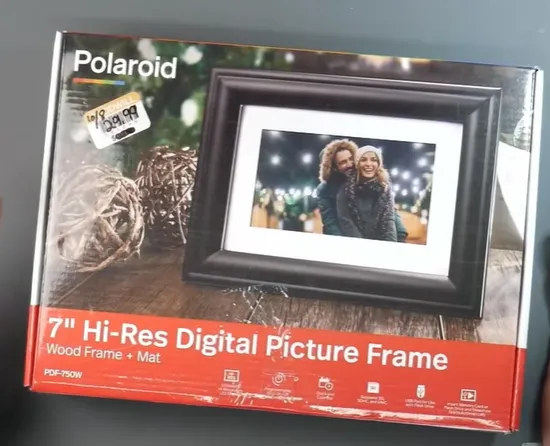
There's something irresistible about a Goodwill find that still powers on. Chase Fournier walked out with a Polaroid 7-inch high-resolution digital picture frame for about fifteen dollars on half-off day. Wood-look frame, mat, nearly 720p screen, SD and USB inputs—the classic early-2010s digital photo frame that once sat on countless shelves cycling family pictures.
Chase already had a Sony frame project on temporary pause because its CPU architecture felt unfamiliar. This Polaroid looked like a better learning platform. He wanted to open it, map the hardware, dump the firmware, and eventually figure out how to run something other than the factory slideshow. No fancy goals of "Doom on a photo frame" yet—just honest curiosity and the desire to understand a real commercial board well enough to talk to it.
That kind of curiosity lives or dies on solid PCB work. The original board is a compact L-shaped multilayer design with tight component placement, an empty NAND footprint that hints at design evolution, and a 4 MB SPI flash that holds the keys. Getting clean access to that flash without destroying the only sample is pure DFM reality: pad integrity, thermal control, and reliable interfacing.
The Cool Moments: From Closed Frame to Readable Strings
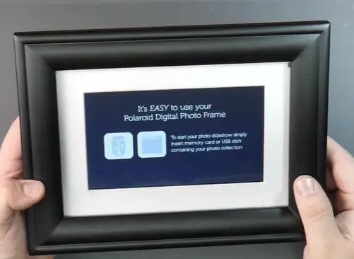
Chase starts the way every good reverse-engineering session should—by powering the unit and watching it behave. The screen comes up, the slideshow runs, the physical buttons still respond. Then the screws come out. Four fasteners release the screen assembly; careful handling keeps fingerprints off the glass. The ribbon cable disconnects cleanly and the L-shaped motherboard is revealed under the microscope.
Figure: Closed Frame Decomposition
Key landmarks appear quickly: the MIPS-based multimedia processor, 3.3 V regulator, USB and SD/MMC connectors, DC power jack (not USB-powered), button-board cable, IR-related pins, and—most interesting—an empty NAND flash pad. The board was clearly designed with the option for more storage that never shipped on this unit.
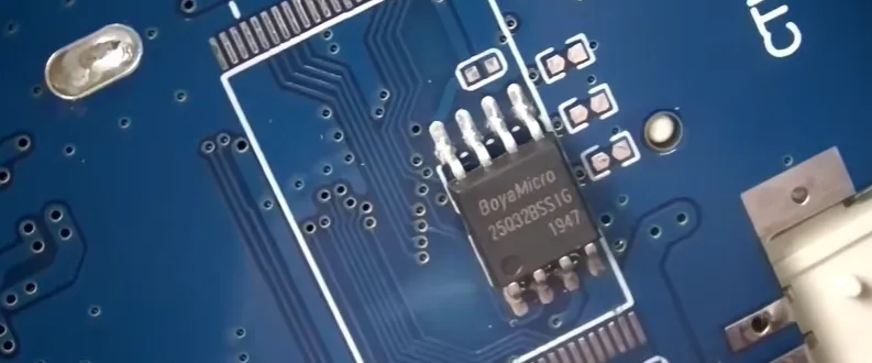
The real prize sits on the reverse side: a 4 MB SPI flash (SOIC package). Chase reflows the pins, lifts the chip with tweezers and an X-Acto knife, and moves it to a small adapter board he has already voltage-modded and prepared. A few careful solder joints later the chip is sitting in a CH programmer / NeoRoger-style reader. The dump runs. Four megabytes land on the desktop as pole_ogg.bin.
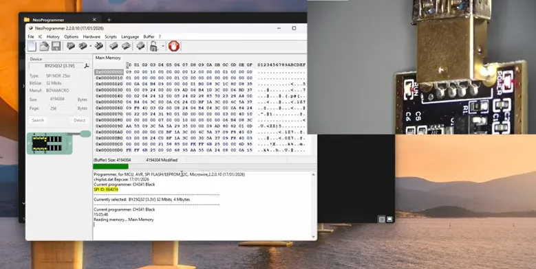
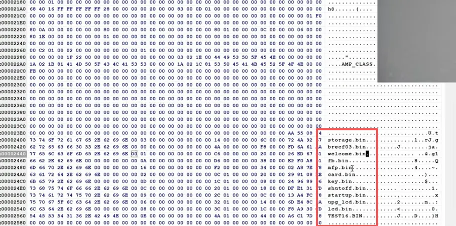
Opening the binary reveals exactly the kind of strings that make a hardware hacker's heart rate climb: storage.bin, welcome.bin, FB.BIN, startup test LCD.bin, "enter debug mode," display enable, speaker on, hard-key shut-off. The firmware is not encrypted. There is a recognizable file system structure. Suddenly the project feels wide open.
Original Board Layout & Key Parameters Observed
Chase's video gives a clear picture of the production board he was working with:
● Form factor: compact L-shaped multilayer PCB designed to fit inside a thin digital frame
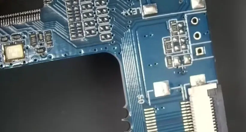
● Processor: MIPS multimedia SoC (exact part still under identification in EP1)
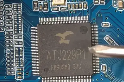
● Non-volatile memory: 4 MB SPI flash (SOIC-8 style package) plus empty NAND footprint
● Power: external DC jack feeding a 3.3 V regulator; no USB power path
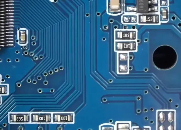
● Interfaces: USB, SD/MMC, screen ribbon, button flex, IR control lines
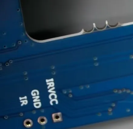
● Surface finish & assembly: typical consumer lead-free solder, fine-pitch parts, no heavy copper or exotic materials
These are classic cost-optimized consumer electronics choices. The empty NAND pad and the accessible SPI flash are the kind of "future-proofing leftovers" that reverse engineers love.
Real Challenges That Showed Up on the Bench
Nothing about reverse-engineering a sealed consumer board is trivial, and Chase hit several classic hurdles that every hardware tinkerer will recognize.
The first big one was getting the SPI flash off cleanly. Reflow, flux, careful lifting with tweezers and an X-Acto—any slip and the pads lift or the chip dies. Once the chip was free, the next problem appeared immediately: he needed to mount it onto a new PCB (the programmer adapter board) so he could read it. The pads on that new board were simply too small. Soldering the fine-pitch flash legs became a real struggle—alignment was tricky and the iron just wouldn't wet the joints reliably.
Figure: SPI flash off and chip mounted onto a new PCB
Chase's solution was pure maker ingenuity. He grabbed another small carrier board, soldered the undersized adapter board onto that larger/more manageable piece, and finally got solid electrical contact. It worked, but it was a classic " this should not have been this hard" moment. The same session also included a quick repair to a voltage-modded pin on the programmer that had been damaged earlier—another reminder that even the tools we use can fight back.
Figure: Grabing another small carrier board, soldered the undersized adapter board onto that larger/more manageable piece.
Other ongoing challenges included locating an unmarked UART on the dense L-shaped board, keeping the fragile screen connector and flex cable intact, and mapping the exact MIPS multimedia processor variant once the strings started appearing. These are the exact pain points that turn a fun Saturday project into a multi-week saga. They also highlight why DFM thinking matters even on the reverse-engineering side: good annular rings, solid pad design, and accessible test points make later analysis far less painful.
How AIVON PCB Made This Project Possible
Here is where the story changes from "clever soldering" to "professional capability."
Chase needed a clean, repeatable way to talk to that 4 MB SPI flash without gambling the original pads every single time. The homemade adapter was good enough for one successful dump, but it was not something you want to rely on for the next ten experiments, for writing modified firmware, or for bringing UART and power monitoring out to proper headers.
That is when a proper custom PCB becomes the real hero of the project.
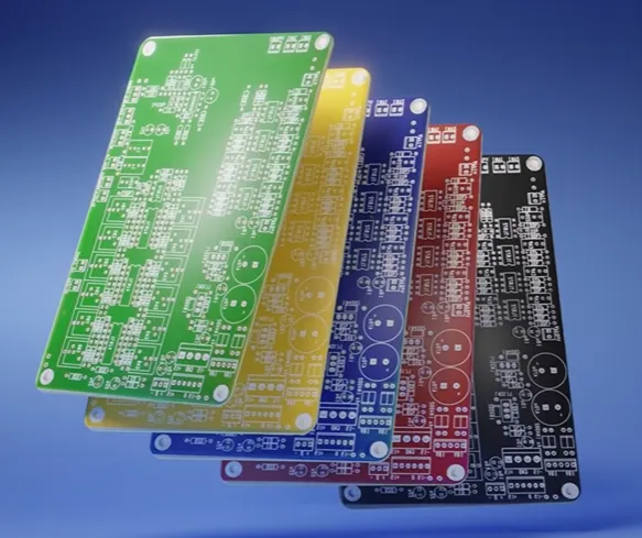
We produced a small, purpose-designed SPI flash breakout and debug interface board for exactly this kind of work. The design goals were simple but non-negotiable:
● Perfect SOIC-8 footprint with generous annular rings so the flash can be soldered and desoldered multiple times without pad failure.
● On-board 100 nF + 10 µF decoupling right at the power pins so the programmer sees a clean rail.
● Level-shifted SPI and optional 3.3 V / 1.8 V selection so the same board works with different programmers.
● Clearly labeled test points and a 2.54 mm header that brings out CLK, MOSI, MISO, CS, and a dedicated UART pair.
● Mechanical strength — 1.0 mm FR-4 with ENIG finish so the board can sit under a microscope or be clipped into a programmer day after day.
AIVON's engineering team ran a full DFM review before the panels were cut. We caught a keep-out violation near the SOIC pads and a slightly undersized via that would have caused yield loss. The boards came back with precise soldermask registration, clean edge plating, and consistent impedance on the short SPI traces.
The difference was immediate. Chase could now remove the original flash once, drop it onto a reliable carrier, and work for hours without worrying about intermittent contact or damaged pads. The same board later became the foundation for permanent debug wiring that will stay with the Polaroid frame through future episodes.
Manufacturing precision mattered. Fast turnaround mattered even more. When a reverse-engineering session is hot, waiting two weeks for boards kills momentum. Getting five perfect adapters in a few days kept the project alive and moving forward.
In short, the original Polaroid board gave Chase the firmware. The AIVON custom PCB gave him a professional, repeatable, and safe way to keep exploring it. That is how a $15 Goodwill find turns into a real hardware platform instead of a one-time lucky dump.
Quick DFM Checklist for Chip-Off & Adapter Projects
|
Item |
Recommendation for this style of work |
|---|---|
|
Annular rings on flash pads |
≥ 0.15 mm after plating to survive rework |
|
Adapter board thickness |
0.8–1.0 mm for mechanical stability under clips |
|
Decoupling on VCC |
100 nF + 10 µF right at the chip pins |
|
Test-point size |
0.8 mm or larger for reliable probe contact |
|
Soldermask clearance |
Extra clearance around fine-pitch SOIC pads |
|
Panelization |
Add mouse-bites or V-score if ordering multiples of the adapter |
Closing the Frame (For Now)
Chase ended EP1 with a successful 4 MB dump and a list of readable strings that already point toward debug modes and file-system structure. The Polaroid is still in pieces, the MIPS core is still being researched, and UART has not yet been located—but the foundation is solid.
That is the real joy of these projects. A cheap consumer board, careful hands, and the ability to spin reliable supporting PCBs when needed turn "I wonder what's inside" into actual progress. If you have a similar frame sitting in a drawer or a new idea that needs a quick adapter board, the path is clearer than it looks. Document everything, respect the original pads, and when you need a clean prototype, treat manufacturing as a partner rather than an afterthought.
The next episode will tell us more about the firmware. Until then, keep the flux flowing and the curiosity high.
FAQ
Q1: What's the safest way to dump an SPI flash from a consumer photo-frame PCB?
A1: Prefer a clip if the package allows it. When desoldering is required, use plenty of flux, controlled hot-air, and a good preheater. Always verify the chip's voltage and pinout against the datasheet before powering the programmer. If you're mounting the chip on a new adapter, double-check pad size first.
Q2: Why do so many cheap digital frames use 2-layer boards and SPI flash?
A2: Cost and simplicity. A 2-layer FR-4 board with a small SPI NOR keeps the BOM under control while still providing enough storage for firmware and a few assets. Multilayer only appears when Wi-Fi, higher resolution, or more complex power domains are needed.
Q3: How can I design a reliable breakout or interposer for future flash work?
A3: Keep the original footprint geometry exact, make the pads generously long (not just minimum), add test points on every SPI line, use a standard header for the programmer side, and request a free DFM review. Castellated edges or a thin rigid board often work well for temporary adapters.
Q4: What surface finish should I choose for prototype boards I'll be reworking a lot?
A4: ENIG is usually the sweet spot—flat, solderable multiple times, and durable. HASL is cheaper but less ideal for fine-pitch or repeated rework.
Q5: Is it worth ordering professional PCBs just for a reverse-engineering fixture?
A5: Absolutely. A clean, labeled adapter board with properly sized pads saves hours of probing and stacking frustration and reduces the risk of damaging the original device. With $1 prototype pricing and fast turnaround, the barrier is low.
Q6: What DFM items should I double-check before sending Gerbers for a photo-frame-style mod board?
A6: Minimum annular ring and especially pad length for the flash footprint, solder-mask dams between fine pads, via-in-pad treatment, outline-to-copper clearance, and any mechanical cutouts that must match the original housing. A good manufacturer will flag undersized pads before fabrication starts.