Watching a late-model PlayStation 3 refuse to stay powered on, then suddenly boot, accept a firmware it was never meant to run, and drop from 4.82 all the way to 3.66 feels like pure science fiction. That is exactly what Chase Fournier delivered in "The Resurrection of My Time Traveling PS3."
One moment the console is power-cycling; the next it is the first documented retail CECH-3000 to successfully travel backward in firmware time. The tool that made it possible was a Raspberry Pi Pico running BadWDSD, carefully wired into the motherboard's XDR RAM and Syscon lines.
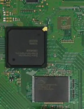
Chase's goal was simple and ambitious at the same time: turn a "locked" 3000-series board into a true time machine capable of running quasi-CFW and freely moving between firmwares that official hardware was never supposed to support. Getting there required more than clever code. It demanded careful attention to how signals travel across a real PCB, how wires survive mechanical stress, and how manufacturing quality keeps an experiment alive after the first rework.
The Console That Refused to Stay Alive
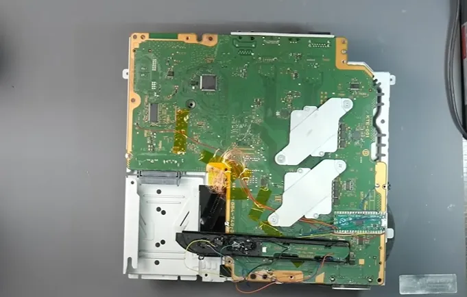
The video opens with a console that powers on, beeps, then immediately shuts down. Chase quickly traces the problem to two critical wires that had worked themselves loose. Those wires carry the XDR CLK and CMD signals the BadWDSD exploit needs to inject code into RAM at the exact right moment. Once they lose solid contact, the entire boot chain collapses.
He switches to slightly thicker enameled wire, burns the insulation clean, adds fresh flux, and re-solders the points under the microscope. A thin coat of UV-curable solder mask locks the runs in place so they cannot migrate again. After a quick isopropyl clean and a corrected NOR flash, the familiar triple beep returns. The Pico LED settles solid, the hard-drive activity light blinks, and the XMB appears on stock 4.82 firmware. That quiet moment of "it actually stayed on" is the first real victory of the build.
Figure: Wires soldering process
Moments That Turned a Mod into a Time Machine
With the hardware stable, Chase demonstrates the feature that gives the project its name. He loads a 3.66 firmware image, holds the recovery button while powering on, and watches the console accept a version that should have been impossible on this board. The install completes, the system reboots, and the classic PlayStation logo appears on 3.66. For the first time a retail 3000 has successfully traveled backward in firmware time.
Figure: 3.66 firmware downloading
The same modchip also enables full qCFW based on Evilnat PEX. Once installed, the console boots with the custom logo, supports most Cobra features, and still allows safe return to official firmware via the BANKSEL pin or a normal PUP reinstall. Optional DEBUG UART access at 576000 baud gives direct Syscon visibility when deeper diagnostics are needed. The user experience feels almost stock until you remember the board was never designed for any of this.
The Quiet Specs That Keep the Exploit Alive
Although the active component is a commercial Raspberry Pi Pico, every successful installation lives or dies by the quality of the connection to the motherboard and the discipline of the supporting layout. The most critical nets are the short, low-inductance CMD and CLK runs. Power and ground need heavier conductors. Any custom carrier board makers later design must respect the same realities.
Typical parameters that keep these builds reliable:
|
Parameter |
Practical Choice |
|---|---|
|
Layers |
2-layer for simple carriers; 4-layer when impedance control is desired |
|
Base material |
FR-4, Tg ≥ 150 °C |
|
Thickness |
0.8–1.6 mm |
|
Copper |
1 oz outer |
|
Surface finish |
ENIG preferred for fine soldering |
|
Signal wire |
0.1 mm magnet wire, kept as short as possible |
|
Power / ground wire |
Noticeably thicker than signal runs |
|
Mechanical retention |
UV solder mask or adhesive strain relief |
When Wires Loosen and Flash Images Go Bad
Even a working install can fail later. Chase's original wires simply vibrated loose over time. Excess length or the wrong gauge on CMD/CLK produces resistance or inductance that prevents XDR RAM initialization, resulting in continuous power cycles or a stubborn green light of death. Measuring roughly 55 Ω to ground after soldering is a quick reality check that many first-time installers skip.
A second failure mode appeared when the NOR backup itself turned out to be corrupt. The console would reach a partial boot state and then stall. Having a verified, checksum-checked backup and the ability to re-flash with an E3-style tool turned a potential brick into a short detour. Flux residue left behind after rework and unsupported wire runs remain the two most common long-term reliability problems on these boards.
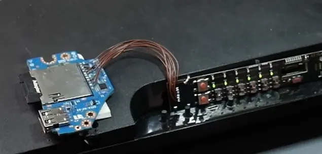
These are classic DFM realities: design for the mechanical environment the board will actually live in, verify every critical image before you trust it, and treat power and signal paths as two different problems.
Practical DFM Checklist for BadWDSD-Style Installs
|
Checkpoint |
Why It Matters |
Target |
|---|---|---|
|
CMD/CLK length and gauge |
XDR timing and RAM init |
≤ 80 mm, 0.1 mm magnet wire |
|
Resistance to ground |
Detect opens or damaged resistors |
≈ 55 Ω |
|
Power and ground wire thickness |
Voltage stability under load |
Heavier than signal wires |
|
Mechanical locking |
Vibration and handling survival |
Solder mask or adhesive |
|
Pre-install NOR backup |
Recovery path if something goes wrong |
Verified checksum, multiple copies |
|
Post-solder cleaning |
Corrosion and leakage risk |
IPA + visual inspection |
How AIVON's Precision PCBs Turned the Vision into a Reliable Reality
Chase's working console proves the exploit and the software stack. Turning that single successful unit into something other makers can actually repeat, improve, and trust required boards that arrive with consistent quality. This is where AIVON's custom PCB manufacturing quietly became the enabling partner.
When builders move beyond a bare commercial Pico and begin designing cleaner RP2040 carriers, better strain-relieved pads, Syscon breakout boards, or experimental interface boards that keep CMD and CLK runs short and well-referenced, they need prototypes that measure correctly the first time. AIVON's quick-turn service delivers exactly that foundation. Controlled stack-ups and higher-Tg FR-4 materials give the thermal stability needed inside a closed console that experiences repeated power cycles. Consistent copper weight and ENIG surface finish produce flat, oxidation-resistant pads that accept fine magnet-wire soldering cleanly and survive multiple rework sessions without lifting or degrading.
Proper via technology and tight manufacturing tolerances keep impedance and inductance low on the critical high-speed nets, directly supporting the narrow timing window the BadWDSD exploit depends on. Responsive DFM feedback catches issues—insufficient clearance around fine pads, unbalanced copper, or inadequate mechanical retention features—before the boards ever leave the factory. The result is a carrier or breakout that simplifies assembly, reduces the chance of intermittent connections, and raises the overall success rate from "it worked once on my bench" to "other people can build this too."
In practical terms, AIVON's boards helped elevate the project beyond a one-off experiment. Cleaner power and ground distribution on a properly manufactured carrier improves voltage stability during the sensitive XDR injection window. Reliable plating and consistent solderability let makers lock wires with solder mask more confidently, addressing the exact mechanical failure Chase had to fix by hand. The manufacturing precision means fewer first-article surprises, so the builder can focus on firmware behavior and recovery paths instead of chasing board-level defects.
What This Build Leaves Behind for the Rest of Us
Chase took a console that refused to stay powered on and turned it into the first retail 3000 capable of genuine firmware time travel. The path ran through careful soldering, short signal runs, verified flash images, and mechanical retention that survives real handling. The same principles scale to any custom board a maker might design around the same exploit.
If you have a wild hardware idea sitting on your desk, start with clean layout practices and a manufacturing partner who treats every prototype as if it has to work the first time. The next console that was never supposed to run custom code might be only one well-made board away.
FAQ
Q1: Why does CMD/CLK wire length and gauge matter so much on the PCB?
A1: These nets carry the high-speed XDR interface used by the exploit. Extra length or the wrong gauge adds inductance and resistance that can prevent proper RAM initialization. Keep runs under 80 mm with 0.1 mm magnet wire and verify roughly 55 Ω to ground after soldering.
Q2: What surface finish is best for fine hand-soldering on a modchip carrier PCB?
A2: ENIG is preferred because it gives a flat, oxidation-resistant surface that accepts fine solder joints cleanly and survives multiple rework cycles without degrading pad quality.
Q3: Should I use a 2-layer or 4-layer PCB for a custom RP2040 BadWDSD carrier?
A3: A well-laid-out 2-layer board is usually sufficient for short signal runs and basic power distribution. Move to 4-layer when you need tighter impedance control, better ground planes, or denser routing around the Pico and connector areas.
Q4: How does solder mask help long-term reliability of the PCB assembly?
A4: A thin, properly cured solder-mask layer locks fine magnet wires in place, prevents them from migrating under vibration, and reduces the chance of accidental shorts. It is one of the simplest and most effective mechanical retention methods for these installs.
Q5: What DFM checks catch the most common failures before a prototype is ordered?
A5: Confirm short critical-signal lengths, adequate copper for power and ground, proper pad sizes for hand soldering, and sufficient clearance around high-speed nets. Requesting manufacturer DFM feedback on these points prevents most first-article problems.
Q6: How important is controlled stack-up and material Tg for boards that live inside a closed console?
A6: Higher Tg FR-4 (≥150 °C) and a consistent stack-up improve thermal stability and reduce the risk of delamination or trace lifting during repeated power cycles and rework. These details matter more than most people expect once the board is sealed inside the chassis.