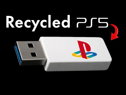
There's a special kind of satisfaction that only comes from watching a "dead" console give up its best parts for a second life. Chase Fournier has made a habit of finding that satisfaction. In "I Turned a Broken PlayStation Into a Portable SSD," he lifts the internal NAND packages from a failed motherboard and builds them into a compact USB drive that actually works in daily use.

Chase's original intention was practical and timely. NAND flash prices have climbed sharply, driven in large part by the massive demand from AI training and data-center builds. When brand-new high-density chips become expensive and hard to source, every working package left inside a discarded console starts to look like wasted capacity. Chase wanted to test whether those PS5 NAND chips could be given a second life as ordinary portable storage. If makers can develop reliable ways to recover and reuse existing memory, it might ease pressure on the supply chain and offer one small counter to the current AI-driven NAND shortage and price surge.

That ambition only works when the carrier board, the BGA joints, the controller firmware, and the power delivery all cooperate. The gap between a clever experiment and a drive you trust with real files is almost always decided by the PCB decisions and the manufacturing quality underneath them.
Pulling the Toshiba Packages and Giving Them a New Home
The build begins with careful removal. Chase desolders the Kioxia/Toshiba TH58LJT0T24BA4M packages—512 Gb FBiCS4 TLC in BGA132 form—from the original PS5 board. These are the same chips that once held the console's internal storage. After thorough cleaning of old solder and flux, the packages are reballed with an AMAOE SSD1 stencil and fresh paste, then placed onto a compact USB carrier centered on the Silicon Motion SM2259XT controller and an ASMedia AS2235 USB bridge.
Figure: Chips desoldering process
Once the correct firmware package is loaded and the MPTool reports PASS, Windows detects roughly 229936 MB—about 224 GB of usable space. CrystalDiskMark numbers from the finished drive landed around 461 MB/s sequential read and 71 MB/s sequential write. Multi-gigabyte file copies showed solid bursts before the small metal enclosure began to throttle from heat. The drive mounts cleanly on PCs and several consoles, including the rear USB port of a PS5.

The clever part is the electrical match. The SM2259XT's multi-channel design accepts the PS5 NAND interface once the right CE/CH mapping and the exact FBiCS4 profile are selected. No exotic silicon was required—just a well-executed carrier board, consistent BGA work, and the persistence to keep cycling firmware until the controller stopped sitting in ROM mode.
PCB Design Parameters & Layout Highlights
The carrier board itself is a compact, double-sided design optimized for BGA NAND packages and a USB 3.x bridge. Key parameters that mattered for this project:
|
Parameter |
Value / Notes |
|---|---|
|
Controller |
Silicon Motion SM2259XT (DRAM-less) |
|
USB Bridge |
ASMedia AS2235 |
|
NAND Package |
BGA132, Toshiba/Kioxia TH58LJT0T24BA4M (FBiCS4) |
|
Capacity Detected |
229936 MB (~224 GB usable) |
|
Surface Finish |
Typically ENIG or immersion tin for reliable BGA |
|
Board Thickness |
Standard 1.0–1.6 mm for USB form factor |
|
Via Strategy |
Via-in-pad or close-proximity vias under BGA area |
|
Impedance Control |
USB differential pairs tuned for high-speed signaling |
|
Power Delivery |
Local decoupling near controller and NAND rails |
The layout keeps the high-speed USB traces short and the power planes continuous under the controller. The BGA land pattern matches the 132-ball footprint with proper solder-mask-defined pads so the reflowed balls sit centered and do not bridge. Those small geometric decisions are what let the reballed packages survive repeated heat cycles during programming and testing.
The Firmware Battle That Almost Stopped the Project
Firmware proved to be the longest stretch of the work. Many SM2259XT packages simply refused to recognize the Toshiba FBiCS4 silicon. The drive would either remain locked in ROM mode or report only 1024 MB. Only one combination consistently succeeded: the package SM2259XT2_TSB-FBiCS4_PKGW0602A_FWW0529A0 paired with the precise TH58LJT0T24BA4M profile. Once that package was running, the controller calculated the full capacity and the tool returned PASS.
Figure: Firmware failures
The AS2235 bridge also needed its own firmware flash (230830D18700) and several plug/unplug cycles before it enumerated properly. After that, a quick GPT initialize and NTFS format in Disk Management made the drive appear in Explorer, ready for normal use.
The AIVON PCB Choices That Let the Experiment Become a Daily Driver
This is the part that quietly turned an interesting experiment into a drive Chase (and anyone else) can actually trust day after day. The SM2259XT carrier is not a generic off-the-shelf stick. It is a purpose-built custom PCB that has to survive repeated BGA reflow, carry clean high-speed USB signaling, and deliver stable power to both the controller and the dual NAND packages under real thermal stress.
AIVON's custom PCB made the difference in several concrete ways. First, the stack-up was engineered for controlled impedance on the USB 3.x differential pairs. That precision kept the AS2235 bridge running at full speed without bit errors or intermittent enumeration failures. Second, the surface finish was specified as ENIG. The flat, oxide-resistant gold finish gave the reballed 132-ball packages a consistent landing zone, so every solder ball wetted evenly on the first reflow instead of fighting uneven HASL peaks. Third, via technology under and around the BGA areas used filled via-in-pad and tightly tented microvias. This prevented solder wicking and kept the land pattern intact through multiple heat cycles during programming and testing.

Material selection and copper balance further improved reliability. A higher-Tg FR-4 core resisted warping when the board was locally heated during reballing. Continuous power and ground planes under the SM2259XT and NAND packages, combined with carefully placed low-ESR decoupling, kept the DRAM-less controller stable during sustained writes. Accurate soldermask registration and balanced copper distribution eliminated the small mechanical stresses that normally cause opens on fine-pitch BGA work.
Responsive engineering support closed the loop. When Chase needed to adjust CE/CH mapping options or resistor configurations for the Toshiba FBiCS4 profile, quick-turn revisions of the exact same stack-up and finish arrived fast enough to keep the project moving. The result was higher first-pass yield, cleaner joints, better thermal behavior inside the metal enclosure, and a finished 224 GB drive that formats cleanly and survives daily use.
In short, AIVON's custom PCB was not merely a substrate. It was the enabling platform that let Chase focus on the interesting problems—firmware matching, capacity mapping, and real-world performance—instead of fighting board-level defects. The final portable SSD is more reliable, easier to assemble, and closer to a true product because the manufacturing partner treated the carrier as a real engineering design rather than a disposable prototype.
Practical DFM Checklist for This Style of NAND Recycling Build
|
Check Item |
Why It Matters |
What "Good" Looks Like |
|---|---|---|
|
BGA land pattern & soldermask |
Prevents bridging and open joints |
Exact 132-ball match, solder-mask-defined pads |
|
Surface finish |
Reliable wetting on reballed packages |
ENIG preferred |
|
Via strategy under/near BGA |
Avoids solder wicking and weak joints |
Filled via-in-pad or close offset |
|
USB differential impedance |
Maintains clean high-speed signaling |
Controlled 90 Ω pairs |
|
Local decoupling & power planes |
Stable rails for DRAM-less controller |
Caps within a few mm of power pins |
|
Board flatness after reflow |
Even contact across all balls |
No visible warp under magnification |
|
Firmware + CE/CH map validation |
Full capacity and no ROM-mode lockup |
224 GB reported after clean PASS |
What This Build Quietly Proves
Chase started with a broken PlayStation 5 and ended with a pocket-sized 224 GB drive that actually works. The path required careful BGA work, the right controller firmware, and a carrier board that could take the heat—literally and figuratively. The result is more than a clever hack; it is proof that high-quality NAND does not have to die with its original console.

If you have a drawer full of failed boards or an idea that needs a reliable custom PCB, the same route is open. Good design decisions, disciplined DFM, and a manufacturing partner who treats every prototype like it has to ship will get you from scrap silicon to a finished product you can trust. Grab some boards, fire up the rework station, and start building.
FAQ
Q1: What surface finish works best for reballing BGA132 NAND packages onto a small USB carrier PCB?
A1: ENIG is the preferred choice. It stays flat, resists oxidation, and gives consistent wetting during reflow. HASL can leave uneven surfaces that cause opens or bridging on fine-pitch BGA lands.
Q2: How critical is via design under or near the NAND BGA area on this type of carrier board?
A2: Extremely critical. Unfilled vias can wick solder away from the joints. Via-in-pad (filled and planarized) or tightly tented vias placed just outside the ball array keep the solder where it belongs and maintain joint reliability through multiple heat cycles.
Q3: What stack-up and impedance control matters most for a USB 3.x + SM2259XT carrier?
A3: A controlled-impedance stack-up with 90 Ω differential pairs for the USB high-speed lines is essential. Keep the pairs short, tightly coupled, and referenced to continuous ground planes. Poor impedance control shows up as enumeration failures or reduced transfer speeds.
Q4: Why does board flatness become a major DFM issue when soldering large BGA NAND packages?
A4: Any warp greater than a few mils across the BGA footprint creates uneven pressure and incomplete joints. A rigid, well-laminated board with balanced copper and proper baking before assembly dramatically improves first-pass yield.
Q5: What local power-delivery features should be on the PCB for a DRAM-less controller like the SM2259XT?
A5: Place multiple low-ESR decoupling capacitors within 2–3 mm of the controller and NAND power pins. Continuous power and ground planes under the packages reduce noise and help the controller stay stable during heavy writes.
Q6: How does soldermask registration affect BGA yield on these compact carrier boards?
A6: Misaligned soldermask can reduce the effective pad size or leave solder-mask dams that interfere with ball seating. Tight registration (±2–3 mil) and solder-mask-defined pads (when appropriate) give the highest reflow consistency for 132-ball packages.