There's something special about watching a maker take a wild idea—an ESP32 that actually understands how you move—and turn it into a polished, battery-powered gadget you can drop in your pocket. That's exactly what happened in the recent How To Electronics project " I Turned an ESP32 into a Motion Tracking Device!" The creator wanted more than another step-counter breakout. He wanted a complete, self-contained IoT activity tracker that could measure steps, cadence, motion intensity, distance, calories, active time, and full roll-pitch-yaw orientation in real time, then serve the data both on a crisp OLED and over a live web dashboard.
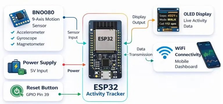
The goal was clear: fuse the powerful onboard sensor fusion of a BNO080-class 9-axis IMU with the Wi-Fi and processing muscle of an ESP32-S3, package everything onto a compact custom board with proper power management, and make it reliable enough for outdoor walking tests. Solid PCB design and manufacturing were never optional. Motion sensors hate noisy ground, battery systems hate voltage droops, and a single-sided dense layout leaves zero room for manufacturing surprises. That's where the real engineering story begins.
What the Tracker Actually Delivers in Real Use
The finished device is surprisingly capable for its size. The BNO085 delivers fused linear acceleration, gyroscope, magnetometer, and rotation-vector data. The ESP32-S3 turns those streams into meaningful fitness metrics: step counting with cadence, estimated distance using different step lengths for walking versus running, a simple calorie model, motion-level percentage, and an activity-mode state machine that cleanly switches between STILL, MOVE, WALK, and RUN.
Figure: The BNO085 chip and its function for activity tracker
Four OLED pages give instant local feedback. Page one is the summary—big step count, current mode, cadence, and a daily goal progress bar. Page two shows distance, calories, active time, and peak g. Page three is live motion. Page four displays roll, pitch, yaw plus the sensor's own accuracy ratings. A single button flips pages on a short press and resets statistics on a long press.
Figure: Four OLED pages give instant local feedback.
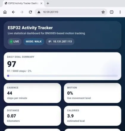
The real "wow" moment for most people is the web dashboard. Once the board joins Wi-Fi, the OLED briefly shows the IP address. Open that address on a phone and you get a modern, responsive interface with live doughnut charts for goal and active-time percentage, a bar-chart snapshot of key metrics, and scrolling trend graphs for cadence and motion level. Watching the graphs climb as you walk faster is genuinely satisfying—and it proves the sensor fusion and processing pipeline are solid.
All of this runs from a single 3.7 V Li-ion cell, charged through a BQ24092, regulated by a TPS63020 buck-boost that keeps 3.3 V stable whether the battery is full or nearly empty. A CP2104 handles USB programming, and the whole power path is tidy enough that outdoor pocket tests work without drama.
Figure: 3.7 V Li-ion cell and type-C USB
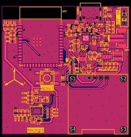
Inside the 4-Layer PCB: Stackup, Layout, and Why It Matters
The board is a deliberate 4-layer design chosen for noise performance and compact single-sided assembly:
|
Parameter |
Specification |
|---|---|
|
Layers |
4 |
|
Stackup |
Top signal + components, L2 solid GND, L3 signal, Bottom signal |
|
Material |
FR-4 |
|
Component side |
Top only (all SMD) |
|
Key interfaces |
I²C (SDA/SCL with 4.7 kΩ pull-ups) for BNO080 + OLED |
|
Power |
Battery + USB-C, BQ24092 charger, TPS63020 3.3 V buck-boost |
|
Programming |
USB-C via CP2104 with auto boot/reset |
|
Display |
0.96″ SSD1306 OLED |
|
Button |
Single active-low with external pull-up |
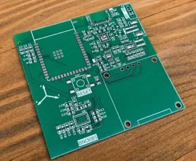
The solid inner ground plane is the quiet hero. It keeps the sensitive BNO080 and the ESP32-S3 RF section happier than a two-layer board ever could. All components live on the top side, which simplifies both hand assembly and future pick-and-place.
Real Hurdles That Showed Up During Development
Turning the schematic into a reliable pocket device surfaced a few classic issues that every motion-tracking board eventually meets.
First was noise on the I²C bus and power rails. The BNO080 is doing continuous sensor fusion; any ground bounce or supply ripple shows up as orientation jitter or step-count glitches. The solid L2 ground plane and careful decoupling placement solved most of it, but only after the layout treated the ground as a continuous sheet rather than a collection of traces.
Second was power integrity across the full battery voltage range. A simple LDO would have dropped out near the end of discharge. The TPS63020 buck-boost keeps 3.3 V rock-solid, but its switching nature required proper inductor selection and layout so the noise never reached the IMU.
Third was mechanical and manufacturing practicality. Everything is on one side in a compact outline. That means silkscreen has to stay clear of pads, vias need consistent treatment, and the board has to survive handling and depanelization without cracking traces near the edge.
I've seen almost identical via-tenting problem on other recent 4-layer FR4 boards. In one case a mixed tenting note versus Gerber data would have left some vias open, inviting solder wicking during HASL and later reliability headaches.
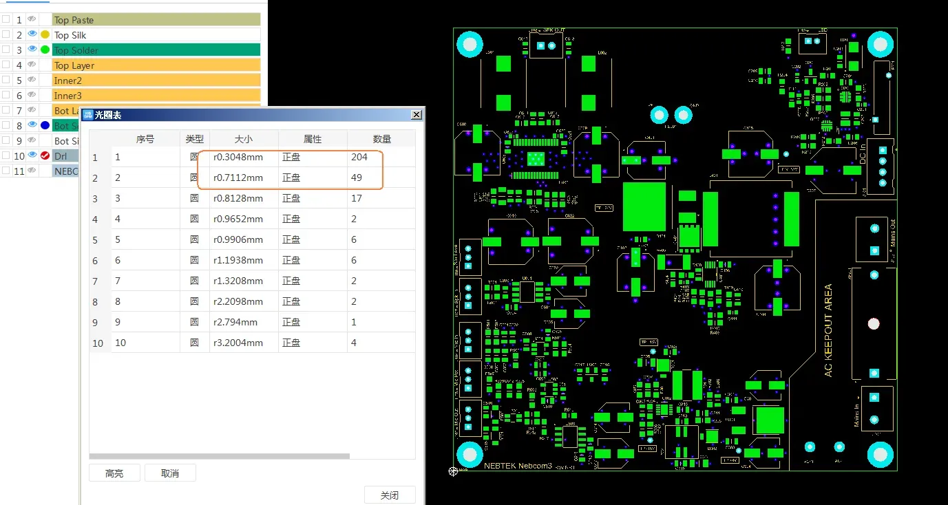
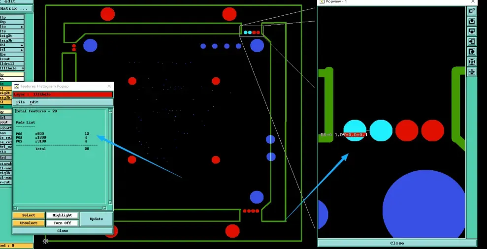
In the silkscreen clearance problem, tight silkscreen near pads and tight stamp-hole spacing on panel breakaways risked both solder issues and premature panel separation. Early DFM catches these before the boards are made—exactly the kind of quiet review that kept this activity tracker's first batch clean.
Assembly itself was straightforward once the boards arrived: all SMD on the top side, battery connector, and a quick USB-C programming session. The real test was outdoor walking with the board in a pocket, watching the web dashboard update cadence and mode in real time. That moment is when the hardware, firmware, and manufacturing decisions all prove they belong together.
How the Custom AIVON Boards Turned the Idea into a Working Prototype
The creator ordered the 4-layer boards from AIVON. A week later a clean box arrived and the quality was immediately obvious—good registration, solid copper, clean solder mask, and a ground plane that actually behaved like a ground plane. That physical board is what let the project move from "works on the bench with flying wires" to "put it in your pocket and walk."
The 4-layer stackup with a dedicated ground layer was the enabler for the sensor performance the creator wanted. Without it, the BNO080 fusion data and the ESP32's Wi-Fi would have fought each other more often. The single-sided component placement simplified hand soldering and left a clean bottom side. Consistent via treatment and legible silkscreen meant no last-minute assembly surprises.
These are the same patterns we see across many compact IoT and wearable boards. A recent 4-layer FR4 job needed careful clarification on full via tenting so solder would not wick into the barrels and create voids or flux traps. Another required silkscreen size and clearance adjustments plus proper breakaway-tab geometry so legends stayed readable and panels survived handling. In both cases the early engineering questions protected yield and long-term reliability. The activity-tracker boards benefited from the same mindset: treat the ground plane as sacred, keep manufacturing notes unambiguous, and design for the actual process the board will see.
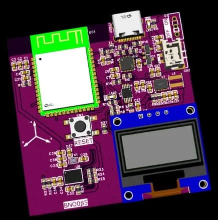
The result is a prototype that feels finished. The OLED pages are crisp, the web charts respond instantly, the battery path is stable, and the whole package is small enough to live in a pocket during real walks. That is the difference a properly manufactured custom PCB makes.
DFM Checklist for Compact 4-Layer Activity-Tracker PCBs
|
Check Item |
Why It Matters for This Design |
Recommended Action |
|---|---|---|
|
Continuous ground plane on L2 |
IMU fusion and Wi-Fi both hate noise |
No signal cuts under critical components |
|
Via tenting consistency |
Prevents solder wicking on dense power/I²C vias |
Explicit full-tent note matching Gerbers |
|
Silkscreen clearance from pads |
Avoids paste or mask interference on single-sided SMT |
Keep ≥0.15 mm, enlarge critical text |
|
Power-plane / decoupling placement |
Stable 3.3 V under battery discharge + switching regulator |
Caps right at ESP32 and BNO080 pins |
|
Antenna keep-out (if module used) |
Maintains Wi-Fi range in pocket use |
Clear copper under antenna region |
|
Breakaway / panel features |
Clean edges after depanelization |
Adequate web strength on mouse bites |
The Real Takeaway from This Build
Watching this ESP32 activity tracker go from schematic to a working, pocketable device is pure maker joy. The creator took a capable IMU, a modern ESP32-S3, thoughtful power management, and a clean 4-layer layout, then pushed it all the way to outdoor testing and a polished web dashboard. The custom PCB was never just a carrier—it was the foundation that made reliable sensor data, stable battery operation, and easy assembly possible.
If you have a similar motion-tracking, wearable, or compact IoT idea sitting in a notebook, the path is clearer than it used to be. Design with a solid ground plane, keep manufacturing notes unambiguous, and partner with a factory that reviews the details before the boards are made. The moment the finished board lights up and starts counting your steps is worth every careful decision.
FAQ
Q1: Why choose a 4-layer board instead of 2-layer for an ESP32 + BNO080 tracker?
A1: A continuous ground plane dramatically reduces noise coupling into the IMU and keeps the ESP32 RF section happier. For a device that lives in a pocket and relies on accurate step and orientation data, the extra layers are almost always worth it.
Q2: What surface finish and solder-mask choices work well for single-sided dense assembly?
A2: Lead-free HASL or ENIG both work; the more important items are consistent via tenting and silkscreen that stays clear of pads so paste and reflow behave predictably.
Q3: How critical is the ground-plane integrity under the BNO080?
A3: Very. Any large cuts or long return paths show up as orientation jitter or false steps. Treat L2 as a solid sheet and stitch vias generously around the sensor.
Q4: Can the same board design support both hand assembly and future SMT production?
A4: Yes—if everything is on one side, the footprints are standard, and the silkscreen and fiducials are clean. The AIVON boards in this project already demonstrated that path.
Q5: What is the most common DFM surprise on compact 4-layer IoT boards like this?
A5: Inconsistent via tenting notes versus Gerber data, and silkscreen that sits too close to pads. Both are easy to catch in a proper pre-production review and expensive if they reach the assembly line.