There's a particular satisfaction when heat suddenly becomes visible on a phone screen. A maker set out to build a compact, battery-powered thermal imaging camera using the MLX90640 far-infrared array and an ESP32. The target was clear: capture a full 32 × 24 temperature matrix (768 points), convert it into a smooth live heatmap with interpolation and color mapping, and stream that image wirelessly from the ESP32's own web server.
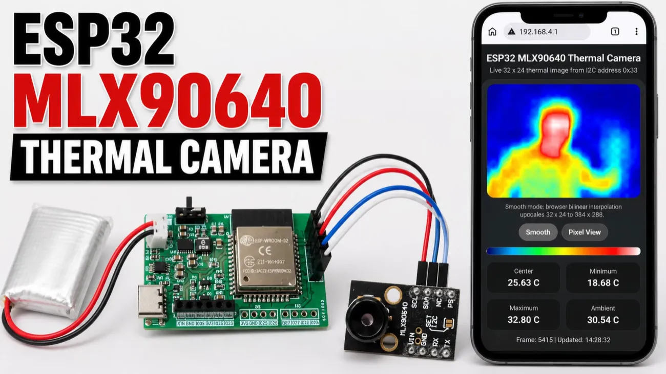
The finished device needed to run from a single LiPo cell, charge cleanly from USB-C, stay small enough to feel handheld, and remain useful for electronics troubleshooting, presence detection or simple thermal monitoring. That only happens when the circuit board is treated as a careful, manufacturable part of the system rather than just a carrier for modules.
From 768 Raw Pixels to a Live Heatmap on Any Phone
Power the board, join the ESP32 Wi-Fi network and open a browser. The raw 32 × 24 matrix appears as a smooth thermal image thanks to bilinear interpolation, frame smoothing, contrast enhancement and selectable color palettes. Hot and cold markers track the extremes while the page continuously shows minimum, maximum, average and center temperatures.
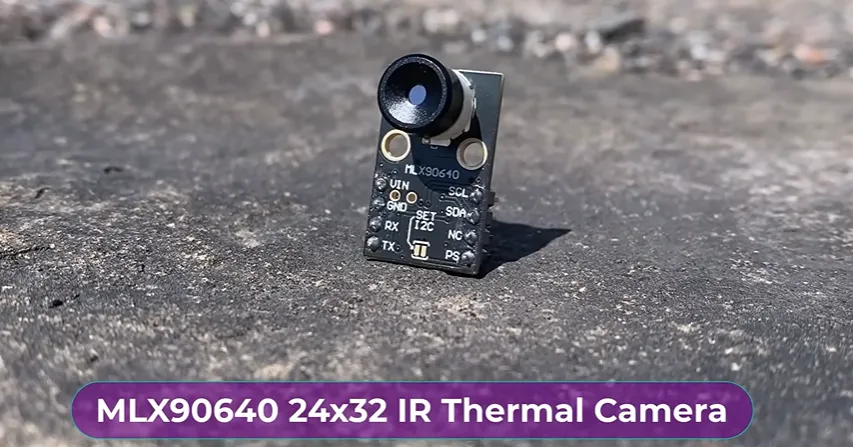
Figure: MLX90640 32×24 IR Array
The MLX90640 itself is a factory-calibrated array in a standard TO39 package. It covers –40 °C to 300 °C with roughly ±1 °C accuracy, offers two field-of-view options, and can run from 0.5 Hz to 64 Hz while drawing less than 23 mA. All of that data is read over I²C, processed on the ESP32 and served in real time. Compared with older 8 × 8 sensors, the higher resolution actually reveals shape and detail instead of just blobs of heat.
Power Path and Front-Side Layout That Kept the Board Practical
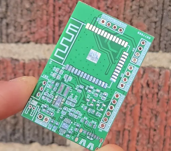
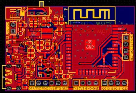
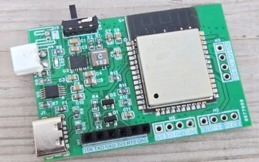
The schematic was drawn in EasyEDA and converted into a compact 2-layer board. All critical components sit on the front side only, which greatly simplifies both hand assembly and visual inspection. The back side is kept clean.
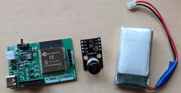
Figure: Front-and-back side PCB layout
Key PCB Design Parameters
|
Parameter |
Specification |
Notes for this project |
|---|---|---|
|
Layers |
2-layer |
Sufficient for power distribution, I²C and control signals |
|
Material |
Standard FR-4 |
Readily available, predictable behaviour |
|
Finished thickness |
1.6 mm (typical) |
Good rigidity for soldering and enclosure |
|
Copper weight |
Standard 1 oz |
Adequate for battery and 3.3 V paths |
|
Surface finish |
Smooth HASL / ENIG class |
Flat pads essential for 0603 + ESP32 module |
|
Component placement |
Front-side only |
All critical parts on top side |
|
Passive package |
0603 |
Compact yet still hand-solderable |
|
Via type |
Through-hole |
Standard reliable plating |
|
Key connectors |
USB-C, JST-PH, PROG header, 4-pin I²C |
Clean interfaces for power, battery, programming and sensor |
|
Special features |
Auto-reset transistors (Q1/Q2), TPS63020 + BQ24092D |
No boot buttons needed; stable 3.3 V across full battery range |
This 2-layer construction is the practical choice for a project of this density and speed. It keeps cost low while still delivering clean power and a solid I²C link to the MLX90640.
First Prototypes and the Real-World Adjustments
The first boards revealed a few practical realities. Minor capacitor and resistor values needed tweaking once the power path and sensor current were measured under real battery conditions. Those changes were locked into the final Gerber so later assemblies required no further correction.
Keeping the MLX90640 quiet is another recurring lesson. The sensor wants a clean 3.3 V rail and a solid I²C bus; any supply noise or ground bounce quickly appears as frame errors. Even on a clean 2-layer board, solder-mask openings and panel features still need attention.
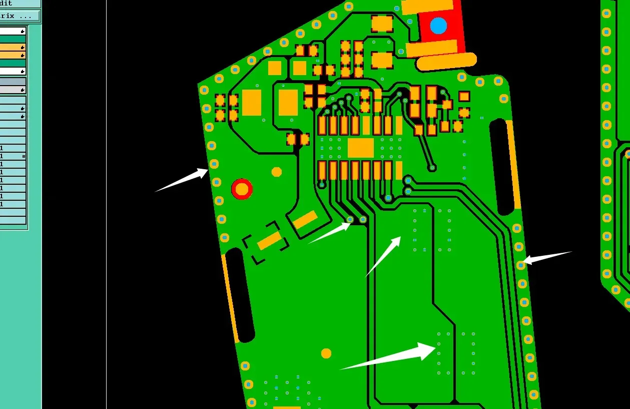
I have seen almost the same PCB solder mask opening design conflict on other 2-layer FR-4 boards. On one recent job the solder-mask Gerber showed mixed openings on vias while the order called for tenting—exactly the kind of conflict that triggers a CAM review. Clarifying which vias should stay open and which should be tented, plus locking compensation on small holes, prevented unintended copper exposure or solder bridges.
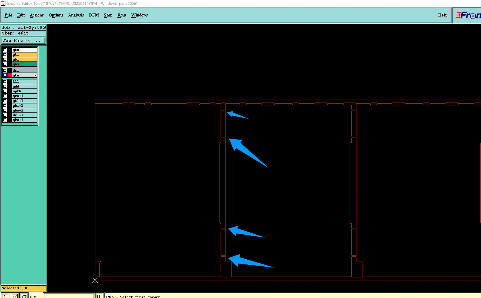
On another 2-layer panel we caught missing stamp holes in solid tabs; without them the boards risked cracking during handling or depanelization. Adding the proper stamp-hole pattern early kept the panels intact through plating, testing and shipping.
Those same early checks on mask definition and mechanical features are what keep a compact thermal-camera board free of the usual prototype surprises.
How AIVON's Boards Turned the Design into a Working Tool
When the final Gerbers were ready, the maker uploaded them, selected standard FR-4 parameters, thickness and solder-mask color, and ordered a small prototype run. About a week later the boards arrived. The quality was excellent—smooth, flat solder pads, precise silkscreen and consistent through-hole plating. That level of finish made the dense front-side 0603 layout and ESP32 module straightforward to assemble by hand. No lifted pads, no bridging from rough plating, no silkscreen that interfered with soldering.
This is where the PCB itself became an enabler rather than a risk. The clean power delivery path (charger + buck-boost) stayed quiet because the copper and plating were consistent. The short I²C runs to the MLX90640 remained solid. The auto-reset circuitry worked on the first upload. In short, the hardware stopped being the limiting factor and the maker could focus on the custom library, the web interface and the interpolation algorithms.
The same manufacturing discipline that protects more complex boards paid off here. On other 2-layer FR-4 jobs we routinely resolve solder-mask opening conflicts (mixed tenting vs open vias, small-hole compensation) during the CAM stage so design intent is preserved. We also catch missing stamp holes on panels before they can cause breakage in handling or depanelization. Applying that same early attention to mask definition, via treatment and panel strength on this thermal-camera board meant the first usable units worked as intended instead of requiring a second spin for basic manufacturability issues.
Because the boards arrived ready to assemble and perform, the project moved from "prototype that almost works" to "tool you can actually carry and trust." The final camera is smaller, cleaner and more reliable than a collection of breakout modules could ever have been.
Compact Thermal-Camera Board DFM Checklist
|
Checkpoint |
Why it matters here |
Practical target |
|---|---|---|
|
Solder-mask openings on vias |
Prevents unintended exposure or solder bridges |
Explicitly state which vias are tented vs open |
|
Stamp holes on panels |
Avoids breakage during handling/depanelization |
Add proper pitch/diameter on solid tabs |
|
Copper-to-hole clearance |
Prevents exposed copper after etch and mask |
≥ 0.25 mm around non-plated holes |
|
Local decoupling |
Keeps the MLX90640 rail quiet |
100 nF + 10 µF right at sensor VDD |
|
I²C routing |
Stable high-speed bus under Wi-Fi load |
Short traces, continuous ground return |
|
Front-side component density |
Reliable hand or simple reflow assembly |
Adequate pad extension, thermal reliefs on large pads |
|
Silkscreen placement |
No mask conflicts on solderable areas |
Keep text clear of pads and vias |
Looking Ahead
What began as a desire to see heat in real time became a practical handheld instrument because the circuit board was designed and manufactured with the same care as the firmware. The maker's power architecture, front-side layout and web-server software found a solid home on a clean 2-layer board, and the finished device simply works.
If you have a thermal, battery-powered or IoT idea waiting in a notebook, the distance from sketch to working prototype is shorter than it looks—provided the board underneath is treated as a precision part of the system. Order a few panels, solder the first unit, and start watching the invisible become visible.
FAQ
Q1: Is a 2-layer board enough for a compact ESP32 + MLX90640 thermal camera, or do I need 4 layers?
A1: For this size and function a well-laid-out 2-layer FR-4 board is usually sufficient. Keep high-current paths short and wide, give the sensor a clean local ground and decoupling, and avoid routing noisy traces under the MLX90640. Four layers help only if you later add high-speed interfaces or much denser routing.
Q2: What surface finish and board thickness work best for hand assembly of 0603 parts and an ESP32 module?
A2: Standard 1.6 mm FR-4 with a smooth HASL or ENIG finish is ideal. Flat, well-plated pads make 0603 soldering and module placement far more reliable. Avoid very thin boards unless mechanical constraints force it—they flex more during hand soldering.
Q3: How do I avoid solder-mask opening conflicts on a 2-layer board?
A3: Clearly state in the fabrication notes which vias should be tented and which should remain open. Also specify whether small vias need zero compensation. Mixed Gerber data versus order defaults is one of the most common triggers for CAM questions on 2-layer boards.
Q4: Do I need stamp holes when ordering a small 2-layer panel?
A4: Yes if the panel uses solid tabs or has zero process edge. Missing stamp holes can cause boards to crack during handling, plating or depanelization. Adding the fabricator’s standard pitch and diameter early prevents that risk.
Q5: Are there specific DFM points that matter most for a battery-powered thermal-sensor board?
A5: Yes—local decoupling right at the sensor, continuous ground return for I²C, thermal reliefs on large pads, clear separation between the switching regulator and the MLX90640, and clean solder-mask definition around vias and pads.
Q6: How can I reduce the chance of needing resistor or capacitor value changes after the first PCB arrives?
A6: Measure the 3.3 V rail under full sensor + Wi-Fi load on a breadboard or early prototype, lock the values, then freeze the Gerber. Small power-path adjustments are normal; documenting them before the final order keeps the next revision clean.