










PCB Prototyping Turns Xbox One eMMC into Reliable Dual-Channel USB Drive
Key Moment
- 0:00 Introduction – Recycling Xbox One eMMC
- 0:35 Plan: Dual eMMC for 10GB Flash Drive
- 1:00 Spare Xbox One S Boards
- 2:00 Removing eMMC Chips with Hot Air
- 2:40 Cleaning the Chips
- 3:00 Testing in eMMC Programmer
- 4:00 Decision to Reball the Chips
- 4:10 PCB Sponsorship
- 5:20 Preparing Solder Paste & Stencil
- 5:50 Reballing the First Chip
- 6:30 Reballing Issues & Fixes
- 8:00 Installing eMMCs on Flash Drive PCB
- 10:00 Final Assembly & Testing
- 12:00 Results & Demonstration
- 14:00 Outro
In a market where memory prices continue to climb and e-waste piles up, makers increasingly look for ways to extract real value from discarded hardware. Chase Fournier's project begins with two failed Xbox One S motherboards. Instead of harvesting the hard drives, he targets the onboard eMMC packages—typically Toshiba or Samsung parts that the console reports as roughly 5 GB usable each. The goal is straightforward yet technically demanding: reball the chips, mount both on a single compact carrier, and produce a functional USB 3.0 flash drive that still performs years after the original consoles died.
This is not a simple salvage exercise. It requires the carrier board itself to support clean BGA reflow, stable dual-channel enumeration, and intact SuperSpeed signaling so sequential performance remains usable. In an era of rising storage costs, the ability to turn scrap silicon into reliable everyday storage has clear appeal for electronics engineers, repair technicians, and makers who refuse to treat old console boards as pure waste.
What This Video Covers
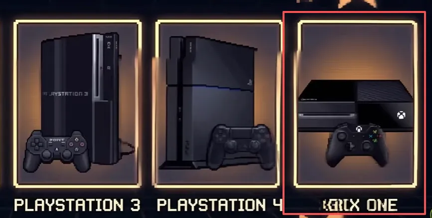
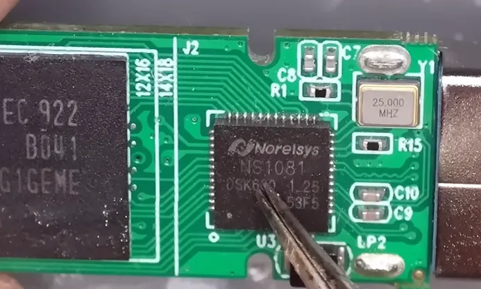
The video walks through every critical stage: hot-air extraction of the eMMC packages, thorough cleaning and programming checks, the iterative reballing process, firmware initialization of the Norelsys NS1081 controller, performance benchmarking with CrystalDiskMark, and real-world mounting tests across a Raspberry Pi cyberdeck, modded Xbox 360, jailbroken PS3, PS4, and finally an Xbox One itself. Viewers see both the moments of success and the exact points where the project nearly failed—failed first reflow, residual tin balls, and the careful recovery steps that ultimately produced a working 10 GB dual-channel drive.
Project Highlights and Key Features
- Dual eMMC packages combined via the NS1081 controller in a RAID-0-style configuration, delivering approximately 10 GB of usable USB 3.0 storage.
- Sequential read speeds near 140 MB/s and write speeds in the 40–64 MB/s range—respectable performance for recycled parts.
- Compact dual-sided carrier layout with carefully length-matched SuperSpeed pairs, continuous ground under high-speed traces, and tight decoupling at both the controller and eMMC power pins.
- Preferred stack-up of 4 layers, 1.0–1.6 mm thickness, 1 oz copper, and ENIG surface finish to ensure flat, oxidation-resistant pads essential for reliable BGA joints.
- Clear pin-1 silk marks, balanced thermal relief, and via strategies that survive multiple hot-air cycles without lifting copper or creating solder-starved pads.
- Proven cross-platform compatibility: the finished drive enumerates cleanly on Linux, multiple console generations, and even the same Xbox One family that originally housed the chips.
Challenges Encountered During Development
The most dramatic obstacles appeared during reballing. On the first reflow attempt, solder balls simply refused to form properly despite added flux. Chase had to lift the chip with tweezers, clean thoroughly, apply a fresh stencil and second layer of paste, and reflow again. Even on the successful second attempt, residual solder floated as free-moving tin balls and required additional flux and careful coaxing to settle into place. A deliberately more distant heat source on the second chip still left residual solder that had to be managed.
These real-world BGA difficulties underscore how sensitive the process is to pad flatness, surface finish quality, and residual oxides. Any uneven plating or poor geometry quickly turns a five-minute install into hours of iterative rework. Impedance control and continuous return paths for the USB SuperSpeed pairs are equally unforgiving; broken ground or unbalanced lengths immediately degrade sequential performance. Without a carrier board that arrives with consistent ENIG, accurate footprints, and a stack-up that actually supports the expected 90 Ω differential impedance, the dual-chip configuration risks intermittent enumeration or complete failure.
How AIVON PCB Helps
This is precisely the class of project where the PCB ceases to be a passive substrate and becomes the quiet enabler of success. AIVON's rapid PCB manufacturing and prototyping service removes the variables that most often derail hand-assembled BGA work. Consistent ENIG finishes provide the flat, oxidation-resistant surface required for clean reballing and reflow. Accurate BGA pad geometry matched to datasheet tolerances reduces opens and tombstoning. Balanced copper and controlled stack-ups deliver the continuous ground planes and impedance targets the NS1081 expects.
Accessible entry pricing for prototypes lets makers iterate without hesitation. Practical engineering feedback on via placement, thermal relief, and decoupling locations further lowers the chance that the board itself becomes the failure point. Clean solder-mask registration around fine-pitch pads and mechanical stability under repeated hot-air cycles mean the focus stays on creative recovery of the eMMC chips rather than fighting fabrication defects. In short, AIVON's one-stop rapid prototyping, expert DFM analysis, and reliable delivery turn an ambitious dual-eMMC concept into a drive that enumerates reliably and sustains 140 MB/s-class sequential performance.
Conclusion
Chase started with two dead Xbox One S boards and finished with a pocket-sized 10 GB USB 3.0 drive that mounts across PCs and multiple console platforms. The journey illustrates both the pure satisfaction of maker-level recycling and the unforgiving realities of BGA rework and high-speed layout. When the carrier board is manufactured to the right DFM standards—ENIG, controlled impedance, proper decoupling, and mechanical robustness—the scrap silicon still has real value left to give.
If you have a drawer of old console boards or a dual-eMMC concept of your own, the same path is open. Respect the DFM details, get a solid prototype in your hands, and see what the silicon can still deliver. Ready to start your next high-reliability carrier or BGA-intensive design? Request a free DFM analysis or instant quote from AIVON PCB today and turn ambitious ideas into boards that actually work.
FAQ
Q1: Why is ENIG preferred over HASL for dual-eMMC carrier boards?
A1: ENIG delivers a flat, oxidation-resistant surface critical for reliable BGA reballing and reflow. HASL is too uneven for fine-pitch eMMC packages and frequently causes incomplete joints or alignment problems during hand assembly.
Q2: Do I really need a 4-layer stack-up for a compact NS1081 USB 3.0 design?
A2: A carefully routed 2-layer board can work for very short SuperSpeed runs, but 4-layer provides continuous ground references, better power distribution, and higher confidence in 90 Ω differential impedance control—especially when two eMMC chips draw current simultaneously.
Q3: What BGA pad and via rules matter most for reballing success?
A3: Match pad size to the eMMC datasheet with modest tolerance, use ENIG finish, keep thermal relief balanced, and place vias so they do not create solder-starved pads. Poor pad geometry or uneven plating is the fastest way to turn a quick install into repeated rework.
Q4: How critical is differential pair matching on these small carriers?
A4: USB SuperSpeed pairs should stay length-matched within a few mils and ride over continuous ground. Even short runs on a dual-eMMC board lose sequential performance if the return path is broken or the pairs are unbalanced.
Q5: What surface-finish and copper-weight combination survives repeated hot-air rework?
A5: 1 oz copper with ENIG is the practical sweet spot. It handles multiple reflow cycles without excessive undercut or warping while still supplying enough current capacity for the NS1081 plus two eMMC devices.
PS3 time. Huh? So, yeah. This is my hacked PS3. This is the one that is running the bad WDSD modded chip. All right, so here's the deal. Console doesn't boot. Turns on, shuts off. I think it's something to do with the mod chip and the wires that have come disconnected. So, let's fix it.
So, according to this diagram, I had these wires soldered up here. I was honestly afraid of breaking them at points on these components here. So, I soldered them up here. This one's still connected and this one... Where did this even... Where did I even solder this to? I honestly don't remember, but it was somewhere anyways. So, these wires need to be unrun and then rerun. I guess we'll start with this one.
All right, so this is one of them. Let's disconnect this wire here. Boom. Let's add a little bit of flux to that point there. And I'm actually going to use some of this thicker wire that's enameled instead. Hopefully, this will serve as a better connection. To be honest, I'm not 100% sure, but it probably will be.
All right, so I'm going to kind of like loosely run the wire over here and then I'll tuck it under some things and then like solder mask it in place. Okay, so let's just cut the wire here like that.
As for the other wire, um dude, I am so sorry for my wiring job. It is atrocious. Oh. Absolutely atrocious, but that's fine. Let's uh come on over here. We'll disconnect this wire from this point here. Come on. There we go. All right, then we'll go back over here. Add a little bit of flux, add some solder. All right, solder our wire. And we're also going to cut this wire right there. That's fine.
All right, now let's run the wires. So, the first one will go under here like that. Right over to this point here right here. So, let's grab the micro pencil micro soldering iron. Solder there. We'll also add some solder to the end of this, burn the enamel on this wire, and then we'll connect the wire. Connect the wire in 3 2... Why am I having trouble? There we go. And then we'll run the second wire. Okay, let's burn the enamel off of this one, and then just like that. That's it. Should be good.
Let's grab a little bit of isopropyl alcohol and a brush, and then grab the old blower and try to clean the board. Blow it away. All right, perfect. That works. All right, let's do that. We'll just add a teensy weensy bit of solder mask to this area. Perfect. Yeah, I would think I would prefer to always add solder mask after you run these wires just because like you don't want them to move from that location. You want them to stay, and that was my problem. They kept falling off. Maybe I was just using wire that was too thick.
All right, let's grab the UV curing light. Oh guys, don't look at this. Just kidding. Grab the UV curing light, you know, the black light, and we'll cure this just like that. All right, perfect. All right, fam. We went ahead and cured this mask.
Okay, so what now? Well, I guess we can we can test the console. We can see if it works.
Have you ever thought about making a PS3 yourself? Well, do I have the solution for you? This video is sponsored by JLCPCB. JLCPCB is a company that delivers high-quality PCBs. So, if you wanted to design your own PS3 PCB motherboard, you can technically do it through KiCad and then send it to JLCPCB, and then they'll make it for you. Now, because JLCPCB is so awesome, they're offering $60 for new users to go towards their PCB prototypes. That means literally you could get your PCB for $1. So, consider trying JLCPCB today for your PCB project.
Let's plug in this hard drive. There we go. Very carefully lift this up like that. Yeah, cuz we can test this outside of the case, I think, without any problems, potentially. Let's grab a piece of paper towel just to insulate the E3 flasher like I was doing with the power supply, the top case that has the E3 flasher attached to it. And then we need the plug to power cord. Let's plug in the power supply. All right, plug in the power cord. 5-volt 5-volt standby, okay. Plugged in.
All right, now we need to move this out of the way. Grab our flasher cable very very very carefully. Grab our flasher and this very very carefully plug in this to the flasher. Very carefully. Don't drop that. All right, beautiful. Okay.
All right, now guys, we should be able to see if the PS3 makes a triple beep when we turn this on. I believe the mod chip worked. Plug this in. All right, wait for this to go solid. All right, and then turn it on. All right, hard drive activity. Oh, it's got my bad. This is This flasher is set to be in fun flash mode, which means it halts the PS3 boot time. Turn that switch off. Now this will be a legit test, okay. Hard drive should read. Beep beep beep beep beep. Is this going to stay on? Guys, I think we did it. We just have to wait and see if we get hard drive activity. We get hard drive activity. Dude, if it was just the two wires and this whole thing works again, that'd be insane.
Console shut down. Uh shoot, what do we try next? Do we try the recovery mode? I don't remember which button I made the recovery mode one. It's either this one or that one. Uh well, I don't know. I guess the only way to try is to plug in the console and hold one of the buttons down. I'm going to guess it's this one. That's not it, all right. Let's try this one. Nope, cuz it didn't auto start. Let's try this one. Yep, that's the recovery mode button. Okay. Now if we continue to hold it, actually I think we're good. 3 4 5 6 7
I think it's fixed, but I'm not 100% sure. So, this red light here is actually the light from the Pico on the bottom of the console. So, the console is getting to a part where it seems like it's working but it's not.
All right, let's try to reflash the NOR chip first. So, the only way to do that is to flip the switch on the flasher, turn it on, the flasher is going to start up and then we can hit the start button, and then this is going to flash the NOR flash on the console. Yeah, so we basically just have to wait until the lights, the progress lights, go all the way to 100% and then it'll be good to go.
Guys, I fixed it. Basically, the NOR flash backup I had on here was corrupt. I fixed the backup, put it back on the SD card, and then flashed it to the console. Now it works.
So, because it works, I want to show you how it works. So, first things first, we have to plug it in. Okay, this LED is the LED that is connected to the pico on the bottom of the console. So, once it stops blinking, go ahead and push power, wait for the triple beep, and the triple beep again. All right. Now, as this turns on, what we're waiting for is the hard drive light to come on, and wait for it, wait for it, and it is flashing. There you go, now you can see it.
All right, let's set the console back down, and we're going to go ahead and focus in over on this monitor over here, which should show the PS3. There we go. So, as you can see, this is a 3000 model PlayStation 3 that has just been exploited with the mod chip. Now, right now this is a current stock 4.82, I believe. So, yes, this is a stock 4.82.
So, what we're going to do is we're going to downgrade this console. Now, this console, as I've said before, is the very first retail...





